Since AMD’s introduction of its newest Zen 3 core for desktop users, the implementation for notebooks and mobile users has been eagerly awaited. In a single generation, on the same manufacturing process, AMD extracted +19% more performance per clock (we verified), so for any system that is power limited, extra performance is often very well received. AMD announced its new Ryzen 5000 Mobile processor family at the start of the year, with processors from 15W to 45W+ in the pipeline, and the first mobile systems coming to market in February. AMD sent us a peak example of Ryzen 5000 Mobile for today’s review, the 35W Ryzen 9 5980HS, as contained in the ASUS ROG Flow X13.
For those that didn’t catch the original announcement a couple of weeks ago, here is a recap of the Ryzen 5000 Mobile family as well as the key points from the announcement.
The Ryzen 5000 Mobile processor series is an upgrade over last year’s Ryzen 4000 Mobile processor series. AMD co-designed both of these processor families to re-use key parts of the chip design, enabling a fast time-to-market and quicker upgrade cycle for AMD’s notebook manufacturing partners (OEMs), like Dell, HP, Lenovo, and others. The major difference between the two processors that most users will encounter is that the new hardware uses eight of AMD’s latest Zen 3 CPU cores, which is an upgrade over the eight Zen 2 cores from last year. The highlight is the +19% raw performance uplift when comparing the two at the same frequency.
Under the hood, there are a few more key changes that enthusiasts will be interested in. The new 8-core Zen 3 design shares a combined 16 MB L3 cache, which enables any of the eight cores to access the full cache, reducing latency to main memory (from 4 MB to 16 MB) compared to the previous design which had two clusters of four Zen 2 cores, each with 4 MB of cache.
The new processor is 180 mm2 in size, compared to 156 mm2 of last generation, but still fits into the same socket. It contains 10.7 billion transistors, which is up from 9.8 billion. This means an effective decrease in transistor density, although we know that Zen 3 cores are slightly larger than Zen 2 cores, and some additional security measures have been added (more on this on the next page).

AMD CEO Dr. Lisa Su Showcasing Ryzen 5000 Mobile at CES
Users may be upset that the new processor range only features Vega 8 graphics, the same as last year’s design, however part of the silicon re-use comes in here enabling AMD to come to market in a timely manner. The Vega 8 design in the previous generation already had a big boost in efficiency and frequency, and this time around we get another +350 MHz on the high-end. Users who want to see RDNA in a mobile processor may have to wait longer. AMD’s re-use strategy may lend itself to changing CPU one generation, GPU the next – we will have to wait and see.
There are other SoC changes, which we will get to later in this review.
The Ryzen 5000 Mobile family is split into two broad product ranges, but both ranges use the same underlying silicon. At the top is the traditional 45 W H-series processors, aimed at productivity notebook designs. For this generation, AMD is pairing the traditional 45 W parts with a range of 35 W ‘HS’ models, optimized for more efficient designs – this will be AMD’s second generation of 35 W ‘HS’ class processors. AMD is also introducing a new range of ‘HX’ processors at 45 W and above which will allow AMD’s partners to co-design high-performance and/or overclockable AMD notebook solutions.
| AMD Ryzen 5000 Mobile: H-Series | |||||||
| AnandTech | Cores Threads |
Base Freq |
Boost Freq |
GPU Cores |
GPU Freq |
TDP | Zen |
| Ryzen 9 5980HX | 8C / 16T | 3300 | 4800 | 8 | 2100 | 45W+ | Zen3 |
| Ryzen 9 5980HS | 8C / 16T | 3000 | 4800 | 8 | 2100 | 35W | Zen3 |
| Ryzen 9 5900HX | 8C / 16T | 3300 | 4600 | 8 | 2100 | 45W+ | Zen3 |
| Ryzen 9 5900HS | 8C / 16T | 3000 | 4600 | 8 | 2100 | 35W | Zen3 |
| Ryzen 7 5800H | 8C / 16T | 3200 | 4400 | 8 | 2000 | 45W | Zen3 |
| Ryzen 7 5800HS | 8C / 16T | 2800 | 4400 | 8 | 2000 | 35W | Zen3 |
| Ryzen 5 5600H | 6C / 12T | 3300 | 4200 | 7 | 1800 | 45W | Zen3 |
| Ryzen 5 5600HS | 6C / 12T | 3000 | 4200 | 7 | 1800 | 35W | Zen3 |
When HS was introduced last year with Ryzen 4000 Mobile, it was an AMD-OEM partnership-only co-designed product requiring AMD approval in order to have access to them. This year however, they seem to be part of the full stack, indicating perhaps that demand for these HS designs was higher than expected.
The new HX models are here to enable high-end gaming, workstation, and desktop-replacement systems, as well as enabling vendors to supply overclockable laptops into the market with sufficient cooling provided. Overclockable laptops isn’t a new concept (Intel has been doing it a while), but it seems that AMD’s partners have requested higher power parts in order to enable this market on AMD. The official TDP for these processors is 45+ W, showcasing that partners can adjust the sustained TDP values north of 45 W if required, likely up to 65 W as needed. In the past, if OEMs wanted to go down this route, they would need to build a portable chassis capable of supporting a desktop processor.
There is some slight deviation from the regular H-series, in that there is no Ryzen 9 standard ‘H’ processor. The Ryzen 7 5800H will sit at the top of that particular market, but the way these numbering systems work means that the Ryzen 7 still has the full eight cores and fast integrated graphics. In that instance, Ryzen 9, with only HS and HX models, are arguably for more ‘specialist’ focused designs.
AMD is advertising the Ryzen 9 5980HS as the best processor for portable gaming performance, while the Ryzen 9 5980HX is ‘the best mobile processor for gaming’. As part of the launch day materials, AMD showcases the Ryzen 9 5980HS as scoring 600 pts in Cinebench R20, which would put it at the same level of performance as AMD’s desktop-class Zen 3 processors. We didn’t quite score 600 in this review with the R9 5980HS (we scored 578).
The traditional 15 W processors, used for ultra-thin and light portable notebooks, form part of the Ryzen 5000 Mobile U-series. AMD is enabling a number of parts with updated Zen 3 cores, but also introducing several processors based on the older Zen 2 design, albeit with updates.
| AMD Ryzen 5000 Mobile: U-Series | |||||||
| AnandTech | Cores Threads |
Base Freq |
Boost Freq |
GPU Cores |
GPU Freq |
TDP | Zen |
| Zen3 | |||||||
| Ryzen 7 5800U | 8C / 16T | 1900 | 4400 | 8 | 2000 | 15W | Zen3 |
| Ryzen 5 5600U | 6C / 12T | 2300 | 4200 | 7 | 1800 | 15W | Zen3 |
| Ryzen 3 5400U | 4C / 8T | 2600 | 4000 | 6 | 1600 | 15W | Zen3 |
| Zen2 | |||||||
| Ryzen 7 5700U | 8C / 16T | 1800 | 4300 | 8 | 1900 | 15W | Zen2 |
| Ryzen 5 5500U | 6C / 12T | 2100 | 4000 | 7 | 1800 | 15W | Zen2 |
| Ryzen 3 5300U | 4C / 8T | 2600 | 3800 | 6 | 1500 | 15W | Zen2 |
The simple way to identify this is with the digit after the number 5. Even digits (5800, 5600, 5400) are based on Zen 3, whereas odd digits (5700, 5500, 5300) are the updated versions of Zen 2. A lot of users will consider these latter processors identical to the previous generation, however we have learned that there are a number of key differences which we will cover in a separate article.
Nonetheless, AMD is promoting the top Ryzen 7 5800U as the company’s most efficient mobile processor to date. Based on a number of enhancements to the silicon design, AMD is claiming a +2hr battery life from a simple processor swap from Ryzen 4000 to Ryzen 5000, even if everything else in the chassis is the same. Nonetheless, AMD is stating that it has worked with controller companies, power delivery suppliers, and notebook designers in order to ensure that those OEMs that want to build systems with more than 20+ hours battery life have the tools to do so. Other OEMs however, particularly for low cost designs or perhaps education models, can freely change the processor from old to new with only a firmware update, as both Ryzen 4000 and Ryzen 5000 are pin compatible.
Overall AMD is claiming 150+ designs with Ryzen 5000 Mobile so far, a significant step up from the 100 designs on Ryzen 4000 Mobile. These are set to include high-end gaming designs with the latest premium graphics cards, a market that AMD has had difficulty breaking into so far.
| AMD Generation Code Names | ||||
| AnandTech | Brand | Core | Graphics | Process Node |
| Mobile Processors | ||||
| Cezanne | Ryzen 5000 Mobile | 8 x Zen 3 | Vega 8 | TSMC N7 |
| Lucienne | Ryzen 5000 Mobile | 8 x Zen 2 | Vega 8 | TSMC N7 |
| Renoir | Ryzen 4000 Mobile | 8 x Zen 2 | Vega 8 | TSMC N7 |
| Picasso | Ryzen 3000 Mobile | 4 x Zen+ | Vega 11 | GF 12nm |
| Raven Ridge | Ryzen 2000 Mobile | 4 x Zen | Vega 11 | GF 14nm |
| Dali | Athlon 3000 | 2 x Zen | Vega 3 | GF 14nm |
| Pollock | ? | 2 x Zen | Vega 3 | GF 14nm |
| Desktop Processors | ||||
| Vermeer | Ryzen 5000 | 16 x Zen 3 | - | TSMC N7 |
| Matisse | Ryzen 3000 | 16 x Zen 2 | - | TSMC N7 |
| Pinnacle Ridge | Ryzen 2000 | 8 x Zen+ | - | GF 12nm |
| Summit Ridge | Ryzen 1000 | 8 x Zen | - | GF 14nm |
| HEDT Processors | ||||
| Genesis Peak | '4th Gen' | Zen 3 | - | ? |
| Castle Peak | Threadripper 3000 | 64 x Zen 2 | - | TSMC N7 |
| Colfax | Threadripper 2000 | 32 x Zen+ | - | GF 12nm |
| Whitehaven | Threadripper 1000 | 16 x Zen | - | GF 14nm |
| Server Processors | ||||
| Genoa | '4th Gen' | Zen 4 | - | ? |
| Milan | EPYC 7003 | 64 x Zen 3 | - | TSMC N7 |
| Rome | EPYC 7002 | 64 x Zen 2 | - | TSMC N7 |
| Naples | EPYC 7001 | 32 x Zen | - | GF 14nm |
Here is a handy table of processor codenames we might use at various parts of these review. These refer to AMD’s internal codenames for the silicon designs, and act as an easier way to talk about the hardware without constantly referring to the branding (especially if certain silicon is used in multiple product ranges).
For this review, AMD supplied the Ryzen 9 5980HS inside the ASUS ROG Flow X13 laptop. It is one of AMD’s key design wins, with a 35 W-grade processor in a sleek design aimed for mobility. As a reviewer who in a normal year spends a lot of time travelling, the specifications on the box make a lot of sense to my regular workflow.
The system features a 13.4-inch 360º hinged display, which as an IPS touchscreen with a 3840x2400 resolution (16:10, finally) running at 120 Hz with adaptive sync, Pantone color certified, and coated in Corning Gorilla Glass. The display is rated for 116% sRGB, 86% Adobe, and 85% DCI-P3.
Under the hood is that AMD Ryzen 9 5980HS processor, with eight Zen 3 cores and sixteen threads, with a 3.0 GHz base frequency and a 4.8 GHz single core turbo frequency, rated at 35 W. ASUS says that they buy the best versions of the 5980HS for the Flow X13 to ensure the best performance and battery life. This processor has Vega 8 graphics, however ASUS has paired it with a GTX 1650 4 GB discrete graphics processor, enabling CUDA acceleration as well as higher performance gaming when needed.

Our unit comes with 32 GB of LPDDR4X-4267 memory, as well as a Western Digital SN350 1TB PCIe 3.0 x4 NVMe storage drive. Both of these would appear to be the standard install for the Flow X13.
ASUS claims the 62 Wh battery is good for 18 hours of use, and the Flow X13 is one of a handful of devices that supports 100 W USB Type-C power delivery. ASUS claims the bundled charger can charge the unit from 0% to 60% in around 39 minutes.
Other features include a back-lit keyboard with consistently sized arrow keys, a full-sized HDMI output as well as a USB 3.2 Gen 2 (10 Gbps) Type-A port, a USB 3.2 Gen 2 (10 Gbps) Type-C ports, a 3.5 mm jack, and a custom PCIe 3.0 x8 output connector for use with ASUS’ XG Mobile external graphics dock. This custom graphics dock can come with a custom designed RTX 3070/3080, and along with graphics power also provides the system with four more USB Type-A ports, HDMI/DP outputs, and Ethernet. With this dock installed, technically the system would have three graphics cards.
All of this comes in at 2.87 lbs / 1.30 Kg, all for under 16mm thick. This is often a key category for both AMD and Intel when it comes to mobility combined with productivity. ASUS has not announced pricing of the ROG Flow X13 yet – the other model in the range is based on the Ryzen 9 5900 HS, but is otherwise identical.
This review is going to be mostly about the processor rather than the Flow X13, due to time constraints (our sample arrived only a few days ago). However, it is worth noting that as with most notebooks, the ROG Flow X13 comes with multiple power and performance modes.
In fact, there are two: Silent and Performance. In each mode there are different values for idle temperature, in order to keep the any audible noise lower, and then different values for power/thermals for turbo and sustained power draw.
These two differ primarily in the sustained power draw and thermal limits:
| ASUS ROG Flow X13 Power Options | ||||||
| AnandTech | Idle Temp* |
Power Instant |
Turbo Power |
Turbo Temp |
Turbo Time |
Sustained |
| Silent | 70ºC | 65 W | 42 W | 85ºC | 6 sec | 15 W @ 68ºC |
| Performance | 65ºC | 65 W | 42 W | 85ºC | 120 sec | 35 W @ 75ºC |
*The idle temperature here is so high, as you'll see later in the review, is because AMD's high-frequency levers are very agressive such that our sensor monitoring tools are activating high frequency modes, despite the small load.
Similar to the launch of Ryzen 4000 Mobile, the unit AMD has supplied us is their top of the line but most efficient H-series processor. For the last generation it was the Ryzen 9 4900HS found in the ASUS ROG Zephyrus G14. The Zephyrus G14 is slightly bigger than the ROG Flow X14 we have today, but the GPU is also better on the G14 (2060 vs 1650). Both processors are rated at 35 W, and both showcase some of the best design AMD wants to lead with at the start of a generation.
The main competition for these processors is Intel’s Tiger Lake. A couple of weeks ago Intel announced its new line of H35 processors, whereby they boost the 15 W U-series processors up to 35 W for additional performance. We have no word on when those units will be in the market (we are told soon), however we have managed to secure an MSI Prestige 14 Evo which contains Intel’s best U-series processor (Core i7-1185G7) and allows for sustained performance at 35 W.
| Comparison Points | ||||
| AnandTech | AMD R9 5980HS |
AMD R9 4900HS |
Intel Core i7-1185G7 |
Intel Core i7-1185G7 |
| Device | ASUS ROG Flow X13 | ASUS ROG Zephyrus G14 | Intel Reference Design | MSI Presige 14 Evo |
| CPU | R9 5980HS | R9 4900HS | i7-1185G7 | i7-1185G7 |
| DRAM | 32 GB LPDDR4-4267 |
16 GB DDR4-3200 |
16 GB LPDDR4-4267 |
16 GB LPDDR4-4267 |
| IGP | Vega 8 | Vega 8 | Iris Xe 64 | Iris Xe 64 |
| dGPU | GTX 1650 | RTX 2060 | - | - |
| Storage | WD SN350 1TB PCIe 3.0 x4 |
Intel 660p 1TB PCIe 3.0 x4 |
Samsung 1TB PCIe 3.0 x4 |
Phison E16 512 GB PCIe 3.0 x4 |
Alongside these numbers we also have historical data from Intel’s Tiger Lake reference platform which ran in 15 W and 28 W modes.
But first, let us discuss the new features in Ryzen 5000 Mobile.
While the introduction page focuses mainly on the change to Zen 3 cores, AMD has explained to AnandTech that there are plenty of other changes in this update which enable both performance and efficiency, as well as battery life enhancements, for users.
From this point on I will start using the silicon codenames, such as
- Cezanne (Ryzen 5000 Mobile with Zen 3),
- Lucienne (Ryzen 5000 Mobile with Zen 2),
- Renoir (Ryzen 4000 Mobile, all Zen 2),
- Vermeer (Ryzen 5000 Desktop, all Zen 3),
- Matisse (Ryzen 3000 Desktop, all Zen 2)
Double Cache and Unified Cache for Cezanne
To reiterate the primary SoC change for Cezanne compared to Renoir, the eight cores now have a unified cache rather than two cache segments. On top of this, the cache size has also doubled.
This is similar to what we saw on the desktop, when AMD introduced Vermeer – Vermeer with Zen 3 had a unified cache over Matisse with Zen 2. At that time, AMD was pointing to the unified cache enabling better gaming performance as it lowered the ‘effective’ latency for CPU memory requests in that combined cache region. The same thing is expected to hold true for the new Cezanne silicon in Ryzen 5000 Mobile, and will play a key part in enabling that +19% IPC increase from generation to generation.
Improved Memory Controller for Cezanne and Lucienne
One of the key metrics in mobile processors is the ability to eliminate excess power overhead, especially when transitioning from an active state to an idle state. All major silicon vendors that build laptop processors work towards enabling super-low power states for when users are idle, because it increases battery life.
A lot of users will be used to features that keep the processor cores in low power states, or the graphics, but also part of this is the interconnect fabric and the memory controller. One of the new developments for Ryzen 5000, and in both Cezanne on Zen 3 and Lucienne on Zen 2, is that AMD has enabled deeper low-power states for the memory physical layer (PHY) interface. This enables the system to save power when the memory subsystem is either not needed or in a period of low activity. This means putting the fabric and memory on its own voltage plane, but also enabling the required logic to drive it to a lower power when idle. AMD states that the low-dropout regulators (LDOs) are configured to enable this transition, and in certain circumstances, allow the PHY to be bypassed to further lower power consumption.
The tradeoff with having a part of the processor in such a low power state is the time it takes to recover from idle, which is also a metric to keep track of. AMD is stating that the design in Ryzen 5000 also enables a fast exit to full activity, meaning that the high performance modes can be entered quickly.
Also on the memory front, it would appear that AMD is doubling capacity support for both LPDDR4X and DDR4. For this generation, Cezanne systems can be enabled with up to 32 GB of LPDDR4X-4267 (68.2 GB/s), or up to 64 GB of DDR4-3200 (51.2 GB/s). The benefits of LPDDR4X are lower power and higher bandwidth, while DDR4 enables higher capacity and a potentially upgradable design.
Per-Core Voltage Control for Cezanne and Lucienne
In line with the same theme of saving power, not only should the periphery of the core be managed for idle use, but the cores should as well. In Ryzen 4000 Mobile, AMD had a system whereby each core could have a separate frequency, which saved some power, but the drawback was that all the cores were on a single voltage plane and so even if a core was idle when another one was heavily loaded, all cores were running at that top voltage. This changes with all members of the Ryzen 5000 Mobile family, as both Cezanne and Lucienne will both feature voltage control on a per-core level.
The slide from AMD shows it best – the cores running at higher frequencies get higher voltage, and the cores that are idling can reduce their voltage to save power. One of the main limits to enabling this sort of profile, aside from actually having the control to do it in the first place, is to do it fast enough for it both to count towards power consumption but also such that it is transparent to the user – the cores should still be able to come to a high voltage/high frequency state within a suitable time. AMD’s design works with operating system triggers and quality of service hooks to apply high-frequency modes in a task-based format.
On AMD’s desktop processors, we saw that the introduction of a feature called CPPC2 helped enable this, and the same is true on the mobile processors, however it took another generation to do the required design and firmware changes.
Power and Response Optimization (CPPC2) for Cezanne and Lucienne
As we accelerate into the future of computing, making the most out of each individual bit of silicon is going to matter more. This means more control, more optimization, and more specialization. For Cezanne and Lucienne, AMD is implementing several CPPC2 features first exhibited on desktop silicon to try and get the most out of the silicon design.
‘Preferred Core’ is a term used mostly on the desktop space to indicate which CPU core in the design can turbo to the highest frequency at the best power, and through a series of operating system hooks, the system will selectively run all single-threaded workloads on that core assuming no other workload is present. Previously, threads could bounce around to enable a more equal thermal distribution – AMD will now selectively keep the workload on the single core until thermal limits kick in, enabling peak performance and no extra delays from thread switching. For overclockable systems, this typically also represents the best core for boosting the frequency, which becomes relevant for Ryzen 5000 Mobile and the new HX series processors.
Another part of CPPC2 is frequency selection, which reduces the time for the transition from low-frequency to high-frequency from 30 milliseconds down to under 2 milliseconds. This equates to a 2-frame adjustment in frequency being reduced down to sub-frame adjustments. The consequences of this enables workloads that occur for shorter than 30 milliseconds can take advantage of a momentarily higher frequency and get completed quicker – it also enables the system to be more responsive to the user, not only in idle-to-immediate environments, but also in situations where power is being distributed across the SoC and those ratios are adjusting for the best performance, such as when the user is gaming. Also enabling load-to-idle transitions on the order of 2 milliseconds improves battery life by putting the processor in a lower power state both quicker and more often, such as between key presses on the keyboard.
The third part of CPPC2 is the migration away from discrete legacy power states within the operating system. With an OS that has a suitable driver (modern Windows 10 and Linux), frequency control of the processor is returned back from the OS to the processor, allowing for finer grained transitions of when performance or power saving is needed. This means that rather than deal with the several power states we used to, the processor has the full continuous spectrum of frequencies and voltages to enable, and will analyze the workflow to decide how that power is distributed (the operating system can give hints to the processor to aid in those algorithms).
GPU Improvements on Cezanne and Lucienne: Vega 8 to Vega 8+
As mentioned on the previous page, one of the criticisms leveled at this new generation of processors is that we again get Vega 8 integrated graphics, rather than something RDNA based. The main reason for this is AMD’s re-use of design in order to enable a faster time-to-market with Zen 3. The previous generation Renoir design with Zen 2 and Vega 8 was built in conjunction with Cezanne to the point that the first samples of Cezanne were back from the fab only two months after Renoir was launched.
If we look at the change in integrated graphics from the start of Ryzen Mobile. The first generation Raven Ridge was built on 14nm, had Vega11 graphics, and had a maximum frequency around 1200 MHz. The graphics in that Renoir design were built on 7nm, and despite the jump down from Vega11 to Vega8, efficiency was greatly increased and frequency had a heathy already a jump up to 1750 MHz. Another generation on to Cezanne and Lucienne, and the graphics gets another efficiency boost, enabling +350 MHz for added performance.
Part of this update is down to tweaks and minor process updates. AMD is able to control the voltage regulation better to allow for new minimums, reducing power, and has enabled a new frequency sensitive prediction model for performance. With the greater power controls on the CPU and SoC side, this means that power budget can be more readily accessible by the integrated graphics, allowing for higher peak power consumption, which also helps boost frequency.
Note that these features apply to both Cezanne and Lucienne, meaning that the Zen 2 products in the Ryzen 5000 Mobile do get a sizeable boost in graphics performance over Renoir here. Ultimately it is that 15 W market for which this update is aimed, given that the H-series (including HS and HX) are likely to be paired with discrete graphics cards.
As and when AMD decides to move from Vega to RDNA, we’re likely going to see some of the Cezanne be re-used such that we might see Zen3 + RDNA in the future, or the combined Zen 4 + GPU chip might be a full upgrade across the board. This is all speculation, but AMD’s CEO Lisa Su has stated that being able to re-use silicon designs like this is a key part of the company’s mobile processor philosophy going forward.
Security Updates in Cezanne
One of the features of Zen 3 is that it enables AMD’s latest generation of security updates. The big update in Zen 3 was the additional of Control Flow Enforcement Technology, known as CET. This is where the processor will create shadow stacks for return calls to ensure that the correct return addresses are called at the end of functions; similarly indirect branch jumps and calls are monitored and protected against should an attacker attempt to modify where an indirect branch is headed.

Both AMD and Intel have spoken about including Microsoft Pluton security in their processors, and we can confirm that neither Cezanne nor Lucienne have Pluton as part of the design. Both AMD and Intel have stated that it will be integrated ‘in the future’, which seems to suggest we may still be another generation or two away.
Process Node Updates on Cezanne and Lucienne
Perhaps one of the smaller updates this time around, but AMD has stated that both Cezanne and Lucienne use the latest intra-process node updates on N7 for these products. While both previous generation Renoir and these two use TSMC’s N7 process, over the lifecycle of the manufacturing node minor changes are made, sometimes to reduce defect density/increase yield, while others might be voltage/frequency updates enabling better efficiency or a skew towards better binning at a different frequency. Usually these additions are minor to the point of not being that noticeable, and AMD hasn’t said much beyond ‘latest enhancements’.
Core-to-Core Latency
As the core count of modern CPUs is growing, we are reaching a time when the time to access each core from a different core is no longer a constant. Even before the advent of heterogeneous SoC designs, processors built on large rings or meshes can have different latencies to access the nearest core compared to the furthest core. This rings true especially in multi-socket server environments.
But modern CPUs, even desktop and consumer CPUs, can have variable access latency to get to another core. For example, in the first generation Threadripper CPUs, we had four chips on the package, each with 8 threads, and each with a different core-to-core latency depending on if it was on-die or off-die. This gets more complex with products like Lakefield, which has two different communication buses depending on which core is talking to which.
If you are a regular reader of AnandTech’s CPU reviews, you will recognize our Core-to-Core latency test. It’s a great way to show exactly how groups of cores are laid out on the silicon. This is a custom in-house test built by Andrei, and we know there are competing tests out there, but we feel ours is the most accurate to how quick an access between two cores can happen.
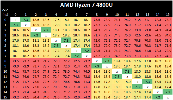
AMD’s move from a dual 4-core CCX design to a single larger 8-core CCX is a key characteristic of the new Zen3 microarchitecture. Beyond aggregating the separate L3’s together for a large single pool in single-threaded scenarios, the new Cezanne-based mobile SoCs also completely do away with core-to-core communications across the SoC’s infinity fabric, as all the cores in the system are simply housed within the one shared L3.
What’s interesting to see here is also that the new monolithic latencies aren’t quite as flat as in the previous design, with core-pair latencies varying from 16.8ns to 21.3ns – probably due to the much larger L3 this generation and more wire latency to cross the CCX, as well as different boost frequencies between the cores. There has been talk as to the exact nature of the L3 slices, whether they are connected in a ring or in an all-to-all scenario. AMD says it is an 'effective' all-to-all, although the exact topology isn't quite. We have some form of mesh with links, beyond a simple ring, but not a complete all-to-all design. This will get more complex should AMD make these designs larger.
Cache-to-DRAM Latency
This is another in-house test built by Andrei, which showcases the access latency at all the points in the cache hierarchy for a single core. We start at 2 KiB, and probe the latency all the way through to 256 MB, which for most CPUs sits inside the DRAM (before you start saying 64-core TR has 256 MB of L3, it’s only 16 MB per core, so at 20 MB you are in DRAM).
Part of this test helps us understand the range of latencies for accessing a given level of cache, but also the transition between the cache levels gives insight into how different parts of the cache microarchitecture work, such as TLBs. As CPU microarchitects look at interesting and novel ways to design caches upon caches inside caches, this basic test proves to be very valuable.
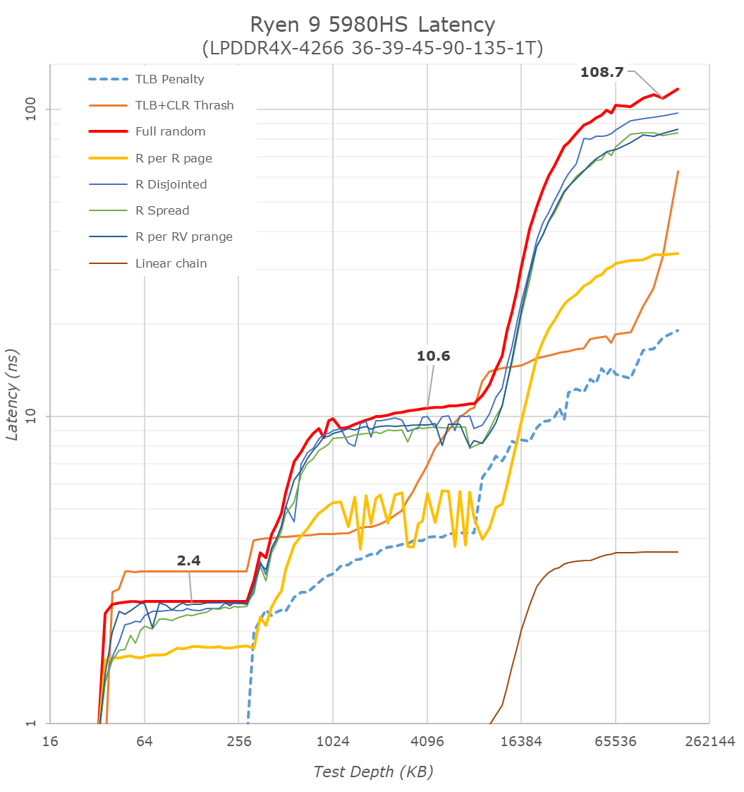
As with the Ryzen 5000 Zen3 desktop parts, we’re seeing extremely large changes in the memory latency behaviour of the new Cezanne chip, with AMD changing almost everything about how the core works in its caches.
At the L1 and L2 regions, AMD has kept the cache sizes the same at respectively 32KB and 512KB, however depending on memory access pattern things are very different for the resulting latencies as the engineers are employing more aggressive adjacent cache line prefetchers as well as employing a brand-new cache line replacement policy.
In the L3 region from 512KB to 16 MB - well, the fact that we’re seeing this cache hierarchy quadrupled from the view of a single core is a major benefit of cache hit rates and will greatly benefit single-threaded performance. The actual latency in terms of clock cycles has gone up given the much larger cache structure, and AMD has also tweaked and changes the dynamic behaviour of the prefetchers in this region.
In the DRAM side of things, the most visible change is again this much more gradual latency curve, also a result of Zen3’s newer cache line replacement policy. All the systems tested here feature LPDDR4X-4266 memory, and although the new Cezanne platform has a slight advantage with the timings, it ends up around 13ns lower latency at the same 128MB test depth point into DRAM, beating the Renoir system and tying with Intel’s Tiger Lake system.
Frequency Ramping
Both AMD and Intel over the past few years have introduced features to their processors that speed up the time from when a CPU moves from idle into a high powered state. The effect of this means that users can get peak performance quicker, but the biggest knock-on effect for this is with battery life in mobile devices, especially if a system can turbo up quick and turbo down quick, ensuring that it stays in the lowest and most efficient power state for as long as possible.
Intel’s technology is called SpeedShift, although SpeedShift was not enabled until Skylake.
One of the issues though with this technology is that sometimes the adjustments in frequency can be so fast, software cannot detect them. If the frequency is changing on the order of microseconds, but your software is only probing frequency in milliseconds (or seconds), then quick changes will be missed. Not only that, as an observer probing the frequency, you could be affecting the actual turbo performance. When the CPU is changing frequency, it essentially has to pause all compute while it aligns the frequency rate of the whole core.
We wrote an extensive review analysis piece on this, called ‘Reaching for Turbo: Aligning Perception with AMD’s Frequency Metrics’, due to an issue where users were not observing the peak turbo speeds for AMD’s processors.
We got around the issue by making the frequency probing the workload causing the turbo. The software is able to detect frequency adjustments on a microsecond scale, so we can see how well a system can get to those boost frequencies. Our Frequency Ramp tool has already been in use in a number of reviews.
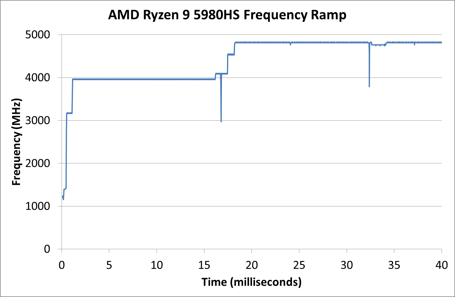
Our frequency ramp showcases that AMD does indeed ramp up from idle to a high speed within 2 milliseconds as per CPPC2. It does take another frame at 60 Hz (16 ms) to go up to the full turbo of the processor mind.
The nature of reporting processor power consumption has become, in part, a dystopian nightmare. Historically the peak power consumption of a processor, as purchased, is given by its Thermal Design Power (TDP, or PL1). For many markets, such as embedded processors, that value of TDP still signifies the peak power consumption. For the processors we test at AnandTech, either desktop, notebook, or enterprise, this is not always the case.
Modern high performance processors implement a feature called Turbo. This allows, usually for a limited time, a processor to go beyond its rated frequency. Exactly how far the processor goes depends on a few factors, such as the Turbo Power Limit (PL2), whether the peak frequency is hard coded, the thermals, and the power delivery. Turbo can sometimes be very aggressive, allowing power values 2.5x above the rated TDP.
AMD and Intel have different definitions for TDP, but are broadly speaking applied the same. The difference comes to turbo modes, turbo limits, turbo budgets, and how the processors manage that power balance. These topics are 10000-12000 word articles in their own right, and we’ve got a few articles worth reading on the topic.
- Why Intel Processors Draw More Power Than Expected: TDP and Turbo Explained
- Talking TDP, Turbo and Overclocking: An Interview with Intel Fellow Guy Therien
- Reaching for Turbo: Aligning Perception with AMD’s Frequency Metrics
- Intel’s TDP Shenanigans Hurts Everyone
In simple terms, processor manufacturers only ever guarantee two values which are tied together - when all cores are running at base frequency, the processor should be running at or below the TDP rating. While manufacturers showcase a rating on the box, motherboard manufacturers often ignore it and use their own settings, based on the motherboard capabilities, making the CPU vendor ratings somewhat useless. The crucial thing is though, the CPU vendors actively encourage the motherboard vendors doing their own thing, creating confusion as to the real power consumption for the workload, and if the frequency on the box is actually what the user is going to get.
For laptops, it gets even worse than desktops. On a laptop, power consumption and frequency control are key parts of the design ethos, however we end up with nested-upon-nested options for power control. While the CPU vendor will have their own power control levels in firmware, the laptop vendor will have another set on top of this in the BIOS, and then the operating system will have another set on top of this, followed by another layer of laptop vendor software. Its turtles all the way down, and each variation produces something quite different.
AMD recommends that all the power levels be left where they are, and the user only controls the vendor software power options. In this case ASUS offers two modes: Silent and Performance. We mentioned these on the first page of this review, and showcased some odd numbers. It might be more striking if I just show the comparison.
To start, I’m simply going to showcase what a full sustained 10 minute CPU load does, first in Performance mode.
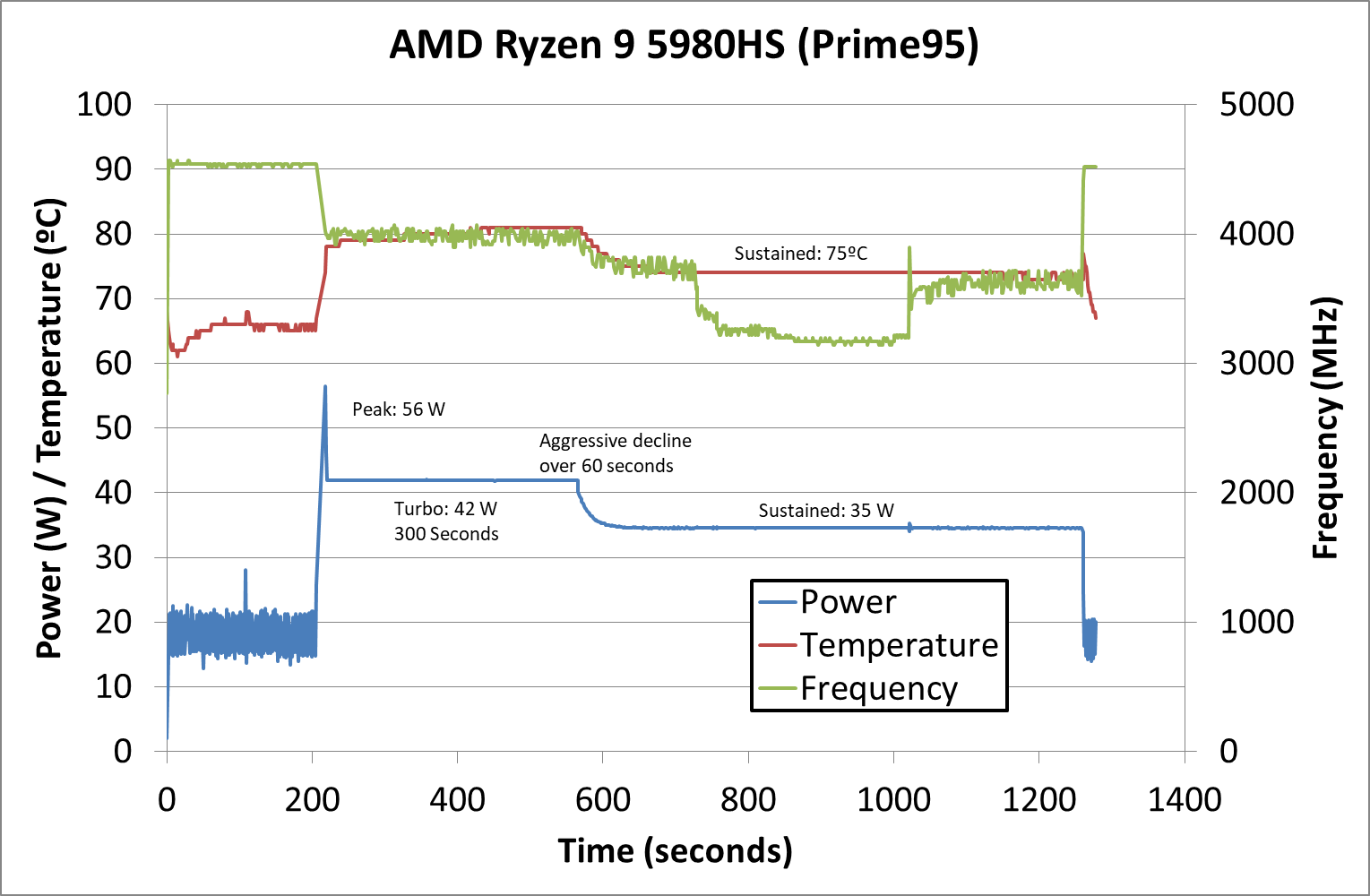
P95 is a heavy AVX workload for this processor, and in performance mode we see the processor peak at 56 W for a couple of seconds, and then hit its turbo mode at 42 W for 300 seconds. During this time we’re around 4000 MHz on all eight cores and sixteen threads, and the system cooling is keeping it around 80ºC. Once the 300 seconds has finished, the system slowly decreases to 35 W and 75ºC over the course of 60 seconds, before hitting a consistent 35 W. The frequency bounces as low as 3200 MHz, likely in line with the instructions from the test.
Now similarly, let’s go to the same benchmark in ‘Silent’ mode.
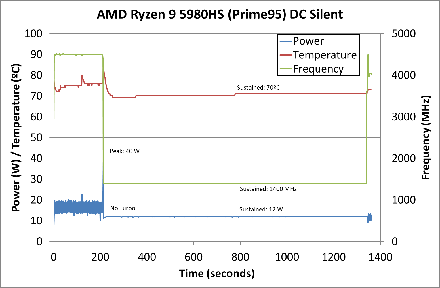
This looks a lot different. Here the system is prioritizing noise over anything else, and that also means reducing voltages and frequencies to the point of absurdity. There is no turbo to speak of in this workload, and the system comes down to 1400 MHz sustained at 70ºC and 12 W. This is still all eight cores, and the system is still quiet, but that is the tradeoff in these designs.
Moving to a more user-friendly workload, Agisoft, which is a mix of ST and MT.
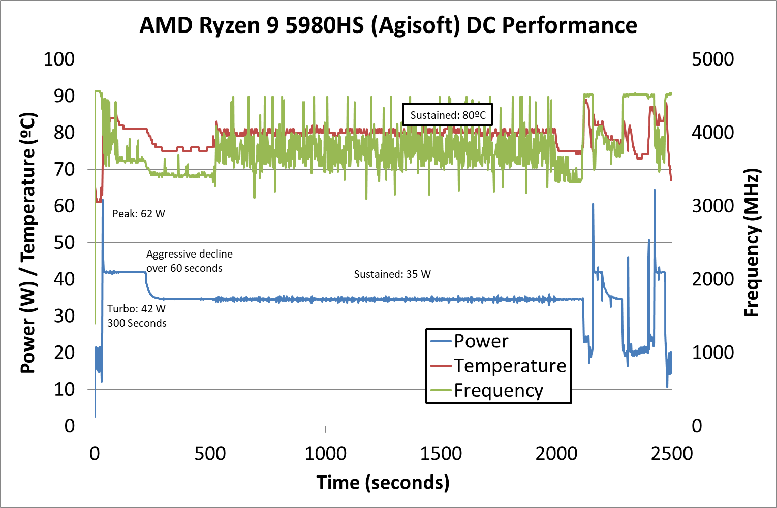
At the start of the test we see the power peak at 62 W for a second or two, before coming down to a 300 second turbo of around 42 W. During this time the frequency comes down to around 3650 MHz, before reducing to 3400 MHz as the turbo budget runs out and the system drops to 35 W for a sustained mode. The second part of the test, which is multi-threaded, starts at around 500 seconds and showcases a sustained temperature of around 81ºC and an opportunistic frequency peaking at 4500 MHz, all while staying at 35 W. Towards the end of the test, as we start looking at single threaded workloads, the system peaks above 60 W on two occasions, but also shows 4500 MHz for ST activity. The CPU temperature rises more to 90ºC as the preferred core is used, but as it is only a single core the thermals are better managed and adjust accordingly.
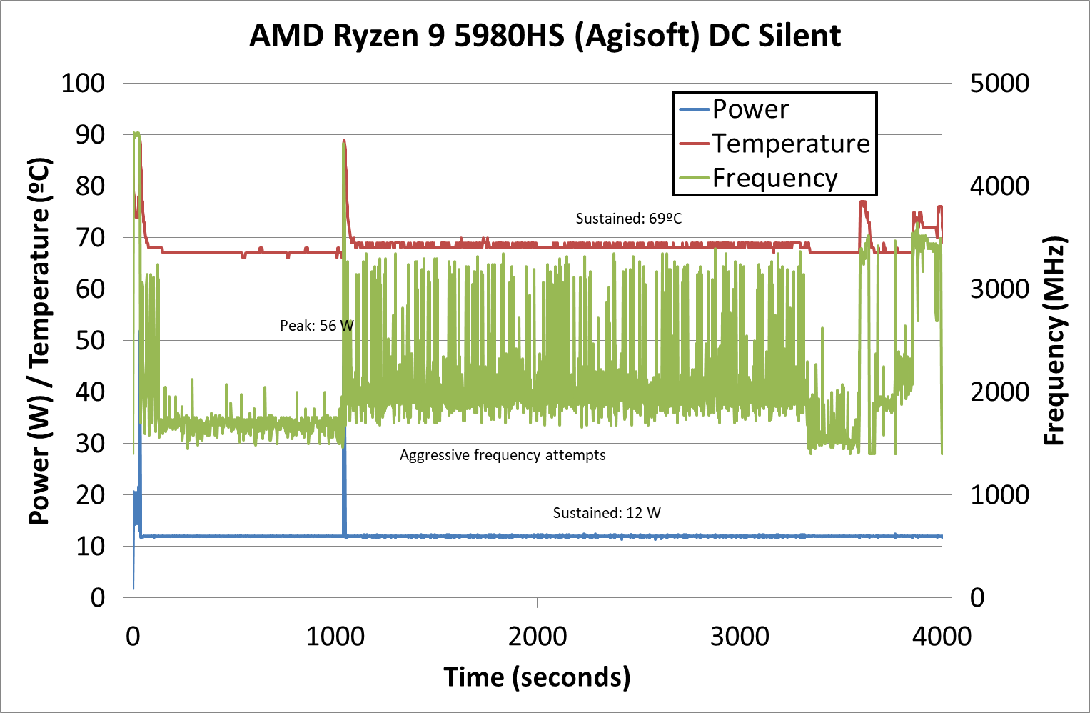
The same workload in silent mode stays at 12 W for almost the entire test. We get a couple of peaks to 56 W, but the system tries to both stay quiet and stay around 68-69ºC by reducing frequency and power. The CPU still tries to remain opportunistic as we can see from the very spikey frequency graph in green, but it is in the region of 1700 MHz to 3300 MHz for most of the test. So while it takes 2443 seconds in performance mode, the same test takes 4059 seconds in silent mode.
This is probably showcasing the worst performance disparity between the two. In a lot of CPU tests, as you’ll see in this review, the differences can be minor. It showcases just how important it is to profile what workload you are running, and keep a close eye on what performance mode the system is running at (there isn’t a clear sign without actively checking the software).
Suffice to say however, in these tests, we do see a peak of 62-65 W on the Ryzen 9 5980HS. It is for all intents and purposes the briefest of spikes, and we don’t necessarily see any thermal increase to the extent that another 10 seconds of workload at 42-45 W does. The sustained turbo mode for 300 seconds is an impressive turbo mode that allows for higher frequencies in most workloads, with only the super sustained tests that might be more at home on a workstation or 15-to-17-inch notebook causing the processor to hit 35 W TDP. It also comes down to thermals, and given the design and temperatures we’re seeing, the ROG Flex 13 is very much a notebook, than a ‘laptop’. Users looking to actually use it on their lap would probably be best creating a thermal profile that keeps the temperature low at the expense of fan noise. When we examine the laptop in further detail, we’ll cover the issue of fan noise.
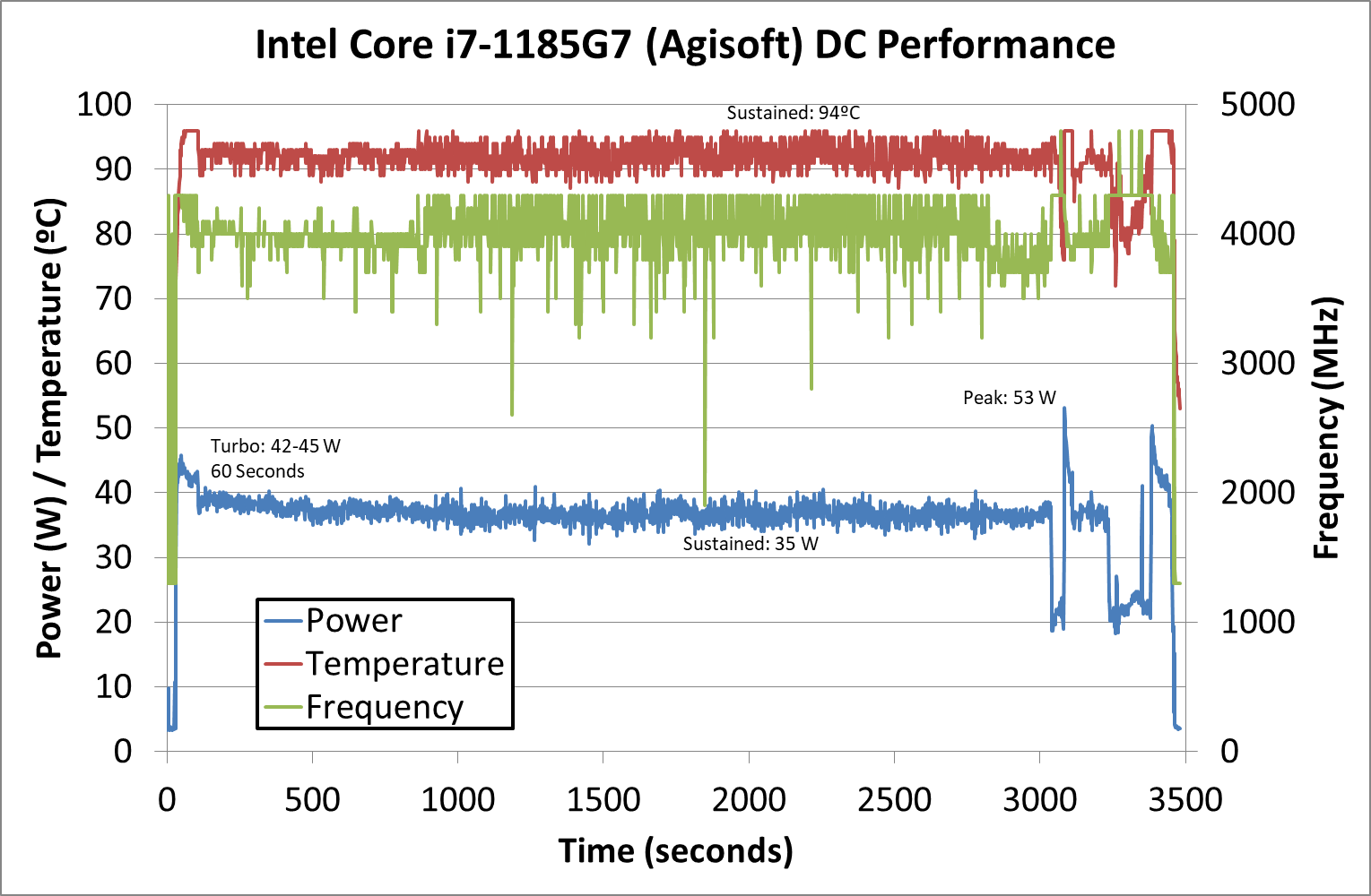
For completeness, here’s the Agisoft graph for the MSI Prestige 14 Evo in performance mode. Intel enables a turbo of 60 seconds, on which we see 42-45 W, although the peak observed is 53 W later in the test. We do see a sustained 35 W mode, averaging around 4000 MHz on all four cores. But what is perhaps worrying is the temperature, being reported as a sustained 92-94ºC on average. That’s quite high. Where the Ryzen 9 5980HS takes 2443 seconds to complete the benchmark, the Intel system takes 3389 seconds.
Our previous set of ‘office’ benchmarks have often been a mix of science and synthetics, so this time we wanted to keep our office section purely on real world performance.
Agisoft Photoscan 1.3.3: link
The concept of Photoscan is about translating many 2D images into a 3D model - so the more detailed the images, and the more you have, the better the final 3D model in both spatial accuracy and texturing accuracy. The algorithm has four stages, with some parts of the stages being single-threaded and others multi-threaded, along with some cache/memory dependency in there as well. For some of the more variable threaded workload, features such as Speed Shift and XFR will be able to take advantage of CPU stalls or downtime, giving sizeable speedups on newer microarchitectures.
For the update to version 1.3.3, the Agisoft software now supports command line operation. Agisoft provided us with a set of new images for this version of the test, and a python script to run it. We’ve modified the script slightly by changing some quality settings for the sake of the benchmark suite length, as well as adjusting how the final timing data is recorded. The python script dumps the results file in the format of our choosing. For our test we obtain the time for each stage of the benchmark, as well as the overall time.
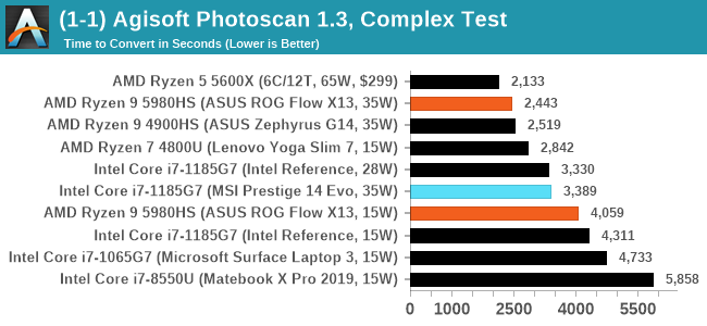
The new Zen 3 system offers a small speed up over the previous generation, and a large lead over the Intel competition here.
Application Opening: GIMP 2.10.18
First up is a test using a monstrous multi-layered xcf file to load GIMP for the first time. While the file is only a single ‘image’, it has so many high-quality layers embedded it was taking north of 15 seconds to open and to gain control on the mid-range notebook I was using at the time. This test is also the run where GIMP optimizes itself, and the optimization requirements scale linearlly with the number of threads in the system.
What we test here is the first run - normally on the first time a user loads the GIMP package from a fresh install, the system has to configure a few dozen files that remain optimized on subsequent opening. For our test we delete those configured optimized files in order to force a ‘fresh load’ each time the software in run. As it turns out, GIMP does optimizations for every CPU thread in the system, which requires that higher thread-count processors take a lot longer to run. So the test runs quick on systems with fewer threads, however fast cores are also needed.

We measure the time taken from calling the software to be opened, and until the software hands itself back over to the OS for user control. The test is repeated for a minimum of ten minutes or at least 15 loops, whichever comes first, with the first three results discarded.
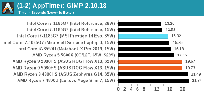
Due to the fast cores and fewer threads, Tiger Lake wins here, but AMD's new processor does offer a good 10% speed up generation over generation.
RISCV Toolchain Compile
Our latest test in our suite is the RISCV Toolchain compile from the Github source. This set of tools enables users to build software for a RISCV platform, however the tools themselves have to be built. For our test, we're running a complete fresh build of the toolchain, including from-stratch linking. This makes the test not a straightforward test of an updated compile on its own, but does form the basis of an ab initio analysis of system performance given its range of single-thread and multi-threaded workload sections. More details can be found here.
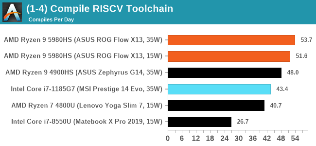
This is a new test, so we are still filling in data points with systems we still have at hand.
In this version of our test suite, all the science focused tests that aren’t ‘simulation’ work are now in our science section. This includes Brownian Motion, calculating digits of Pi, molecular dynamics, and for the first time, we’re trialing an artificial intelligence benchmark, both inference and training, that works under Windows using python and TensorFlow. Where possible these benchmarks have been optimized with the latest in vector instructions, except for the AI test – we were told that while it uses Intel’s Math Kernel Libraries, they’re optimized more for Linux than for Windows, and so it gives an interesting result when unoptimized software is used.
3D Particle Movement v2.1: Non-AVX and AVX2/AVX512
This is the latest version of this benchmark designed to simulate semi-optimized scientific algorithms taken directly from my doctorate thesis. This involves randomly moving particles in a 3D space using a set of algorithms that define random movement. Version 2.1 improves over 2.0 by passing the main particle structs by reference rather than by value, and decreasing the amount of double->float->double recasts the compiler was adding in.
The initial version of v2.1 is a custom C++ binary of my own code, and flags are in place to allow for multiple loops of the code with a custom benchmark length. By default this version runs six times and outputs the average score to the console, which we capture with a redirection operator that writes to file.
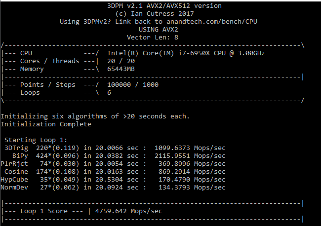
For v2.1, we also have a fully optimized AVX2/AVX512 version, which uses intrinsics to get the best performance out of the software. This was done by a former Intel AVX-512 engineer who now works elsewhere. According to Jim Keller, there are only a couple dozen or so people who understand how to extract the best performance out of a CPU, and this guy is one of them. To keep things honest, AMD also has a copy of the code, but has not proposed any changes.
The 3DPM test is set to output millions of movements per second, rather than time to complete a fixed number of movements.
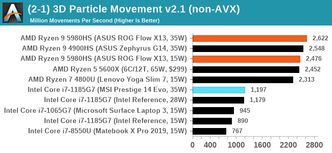
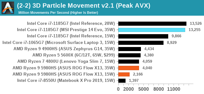
Intel's Tiger Lake has AVX-512 units, which is why they are so far ahead in the peak AVX test. For AMD vs AMD, we're seeing around the same score between the previous generation Zephyrus and the new Flow X13, however in multithreaded the Flow X13 seems to regress slightly.
y-Cruncher 0.78.9506: www.numberworld.org/y-cruncher
If you ask anyone what sort of computer holds the world record for calculating the most digits of pi, I can guarantee that a good portion of those answers might point to some colossus super computer built into a mountain by a super-villain. Fortunately nothing could be further from the truth – the computer with the record is a quad socket Ivy Bridge server with 300 TB of storage. The software that was run to get that was y-cruncher.
Built by Alex Yee over the last part of a decade and some more, y-Cruncher is the software of choice for calculating billions and trillions of digits of the most popular mathematical constants. The software has held the world record for Pi since August 2010, and has broken the record a total of 7 times since. It also holds records for e, the Golden Ratio, and others. According to Alex, the program runs around 500,000 lines of code, and he has multiple binaries each optimized for different families of processors, such as Zen, Ice Lake, Sky Lake, all the way back to Nehalem, using the latest SSE/AVX2/AVX512 instructions where they fit in, and then further optimized for how each core is built.

For our purposes, we’re calculating Pi, as it is more compute bound than memory bound. In single thread mode we calculate 250 million digits, while in multithreaded mode we go for 2.5 billion digits. That 2.5 billion digit value requires ~12 GB of DRAM, and so is limited to systems with at least 16 GB.
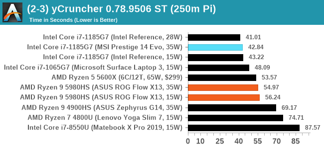
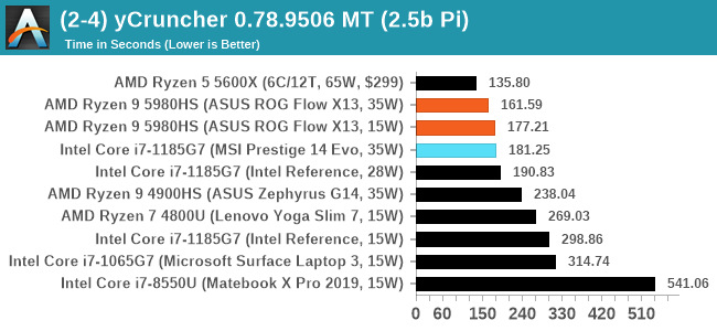
Intel here again benefits from AVX-512, however for a big multithreaded test, the eight cores of AMD pushes it ahead. Compared to the previous generation AMD processor, we see significant speedups for both ST and MT, showcasing the benefits of the new Zen 3 core and cache system.
NAMD 2.13 (ApoA1): Molecular Dynamics
One of the popular science fields is modeling the dynamics of proteins. By looking at how the energy of active sites within a large protein structure over time, scientists behind the research can calculate required activation energies for potential interactions. This becomes very important in drug discovery. Molecular dynamics also plays a large role in protein folding, and in understanding what happens when proteins misfold, and what can be done to prevent it. Two of the most popular molecular dynamics packages in use today are NAMD and GROMACS.
NAMD, or Nanoscale Molecular Dynamics, has already been used in extensive Coronavirus research on the Frontier supercomputer. Typical simulations using the package are measured in how many nanoseconds per day can be calculated with the given hardware, and the ApoA1 protein (92,224 atoms) has been the standard model for molecular dynamics simulation.
Luckily the compute can home in on a typical ‘nanoseconds-per-day’ rate after only 60 seconds of simulation, however we stretch that out to 10 minutes to take a more sustained value, as by that time most turbo limits should be surpassed. The simulation itself works with 2 femtosecond timesteps. We use version 2.13 as this was the recommended version at the time of integrating this benchmark into our suite. The latest nightly builds we’re aware have started to enable support for AVX-512, however due to consistency in our benchmark suite, we are retaining with 2.13. Other software that we test with has AVX-512 acceleration.
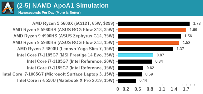
NAMD also sees good speedups, and the eight core mobile processor is within reach of that six-core desktop processor. Intel lags behind on the 2.13 version, as we wait for the AVX-512 to come out of alpha versions of the software.
AI Benchmark 0.1.2 using TensorFlow: Link
Finding an appropriate artificial intelligence benchmark for Windows has been a holy grail of mine for quite a while. The problem is that AI is such a fast moving, fast paced word that whatever I compute this quarter will no longer be relevant in the next, and one of the key metrics in this benchmarking suite is being able to keep data over a long period of time. We’ve had AI benchmarks on smartphones for a while, given that smartphones are a better target for AI workloads, but it also makes some sense that everything on PC is geared towards Linux as well.
Thankfully however, the good folks over at ETH Zurich in Switzerland have converted their smartphone AI benchmark into something that’s useable in Windows. It uses TensorFlow, and for our benchmark purposes we’ve locked our testing down to TensorFlow 2.10, AI Benchmark 0.1.2, while using Python 3.7.6.

The benchmark runs through 19 different networks including MobileNet-V2, ResNet-V2, VGG-19 Super-Res, NVIDIA-SPADE, PSPNet, DeepLab, Pixel-RNN, and GNMT-Translation. All the tests probe both the inference and the training at various input sizes and batch sizes, except the translation that only does inference. It measures the time taken to do a given amount of work, and spits out a value at the end.
There is one big caveat for all of this, however. Speaking with the folks over at ETH, they use Intel’s Math Kernel Libraries (MKL) for Windows, and they’re seeing some incredible drawbacks. I was told that MKL for Windows doesn’t play well with multiple threads, and as a result any Windows results are going to perform a lot worse than Linux results. On top of that, after a given number of threads (~16), MKL kind of gives up and performance drops of quite substantially.
So why test it at all? Firstly, because we need an AI benchmark, and a bad one is still better than not having one at all. Secondly, if MKL on Windows is the problem, then by publicizing the test, it might just put a boot somewhere for MKL to get fixed. To that end, we’ll stay with the benchmark as long as it remains feasible.
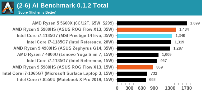
There's a good jump for AMD here generation-on-generation, pushing it ahead of Tiger Lake. At 15 W however, Intel would seem to have the upper hand.
Simulation and Science have a lot of overlap in the benchmarking world, however for this distinction we’re separating into two segments mostly based on the utility of the resulting data. The benchmarks that fall under Science have a distinct use for the data they output – in our Simulation section, these act more like synthetics but at some level are still trying to simulate a given environment.
DigiCortex v1.35: link
DigiCortex is a pet project for the visualization of neuron and synapse activity in the brain. The software comes with a variety of benchmark modes, and we take the small benchmark which runs a 32k neuron/1.8B synapse simulation, similar to a small slug.
The results on the output are given as a fraction of whether the system can simulate in real-time, so anything above a value of one is suitable for real-time work. The benchmark offers a 'no firing synapse' mode, which in essence detects DRAM and bus speed, however we take the firing mode which adds CPU work with every firing.

The software originally shipped with a benchmark that recorded the first few cycles and output a result. So while fast multi-threaded processors this made the benchmark last less than a few seconds, slow dual-core processors could be running for almost an hour. There is also the issue of DigiCortex starting with a base neuron/synapse map in ‘off mode’, giving a high result in the first few cycles as none of the nodes are currently active. We found that the performance settles down into a steady state after a while (when the model is actively in use), so we asked the author to allow for a ‘warm-up’ phase and for the benchmark to be the average over a second sample time.
For our test, we give the benchmark 20000 cycles to warm up and then take the data over the next 10000 cycles seconds for the test – on a modern processor this takes 30 seconds and 150 seconds respectively. This is then repeated a minimum of 10 times, with the first three results rejected. Results are shown as a multiple of real-time calculation.
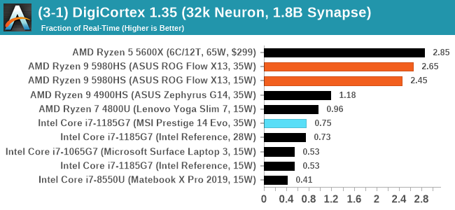
DigiCortex seems to have taken a shine to Zen 3, especially processors with a single chiplet of cores. Intel can't seem to compete here.
Dwarf Fortress 0.44.12: Link
Another long standing request for our benchmark suite has been Dwarf Fortress, a popular management/roguelike indie video game, first launched in 2006 and still being regularly updated today, aiming for a Steam launch sometime in the future.
Emulating the ASCII interfaces of old, this title is a rather complex beast, which can generate environments subject to millennia of rule, famous faces, peasants, and key historical figures and events. The further you get into the game, depending on the size of the world, the slower it becomes as it has to simulate more famous people, more world events, and the natural way that humanoid creatures take over an environment. Like some kind of virus.
For our test we’re using DFMark. DFMark is a benchmark built by vorsgren on the Bay12Forums that gives two different modes built on DFHack: world generation and embark. These tests can be configured, but range anywhere from 3 minutes to several hours. After analyzing the test, we ended up going for three different world generation sizes:
- Small, a 65x65 world with 250 years, 10 civilizations and 4 megabeasts
- Medium, a 127x127 world with 550 years, 10 civilizations and 4 megabeasts
- Large, a 257x257 world with 550 years, 40 civilizations and 10 megabeasts
DFMark outputs the time to run any given test, so this is what we use for the output. We loop the small test for as many times possible in 10 minutes, the medium test for as many times in 30 minutes, and the large test for as many times in an hour.
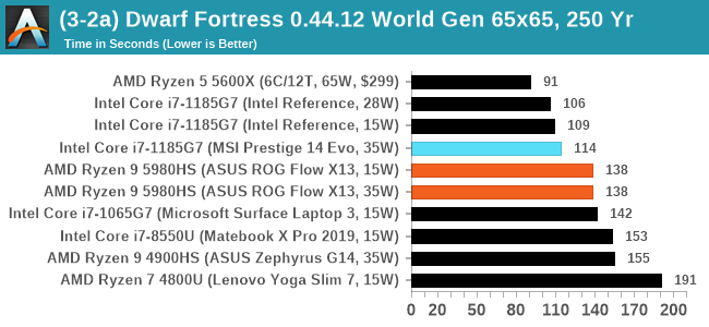
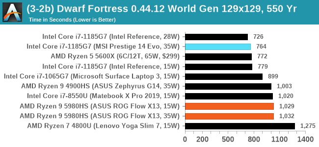
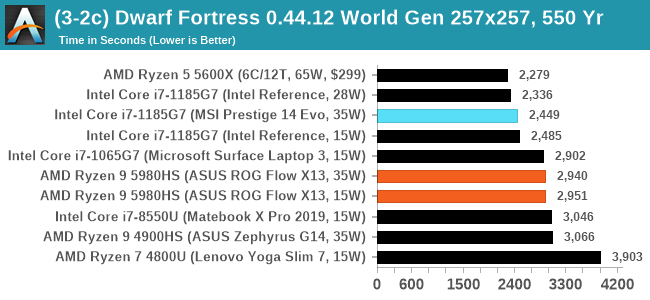
DF has historically been an Intel favorite, and we're not seeing much of a speedup for mobile Zen 3 over mobile Zen 2 here.
Dolphin v5.0 Emulation: Link
Many emulators are often bound by single thread CPU performance, and general reports tended to suggest that Haswell provided a significant boost to emulator performance. This benchmark runs a Wii program that ray traces a complex 3D scene inside the Dolphin Wii emulator. Performance on this benchmark is a good proxy of the speed of Dolphin CPU emulation, which is an intensive single core task using most aspects of a CPU. Results are given in seconds, where the Wii itself scores 1051 seconds.
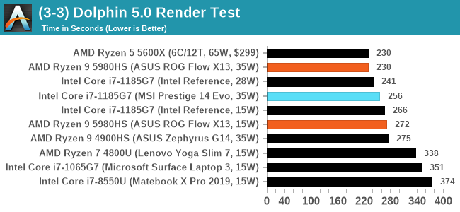
The 35W variant of Cezanne pushes through here, matching the desktop processor, and a sizeable performance jump over the previous generation Renoir.
Rendering tests, compared to others, are often a little more simple to digest and automate. All the tests put out some sort of score or time, usually in an obtainable way that makes it fairly easy to extract. These tests are some of the most strenuous in our list, due to the highly threaded nature of rendering and ray-tracing, and can draw a lot of power. If a system is not properly configured to deal with the thermal requirements of the processor, the rendering benchmarks is where it would show most easily as the frequency drops over a sustained period of time. Most benchmarks in this case are re-run several times, and the key to this is having an appropriate idle/wait time between benchmarks to allow for temperatures to normalize from the last test.
Blender 2.83 LTS: Link
One of the popular tools for rendering is Blender, with it being a public open source project that anyone in the animation industry can get involved in. This extends to conferences, use in films and VR, with a dedicated Blender Institute, and everything you might expect from a professional software package (except perhaps a professional grade support package). With it being open-source, studios can customize it in as many ways as they need to get the results they require. It ends up being a big optimization target for both Intel and AMD in this regard.
For benchmarking purposes, we fell back to one rendering a frame from a detailed project. Most reviews, as we have done in the past, focus on one of the classic Blender renders, known as BMW_27. It can take anywhere from a few minutes to almost an hour on a regular system. However now that Blender has moved onto a Long Term Support model (LTS) with the latest 2.83 release, we decided to go for something different.

We use this scene, called PartyTug at 6AM by Ian Hubert, which is the official image of Blender 2.83. It is 44.3 MB in size, and uses some of the more modern compute properties of Blender. As it is more complex than the BMW scene, but uses different aspects of the compute model, time to process is roughly similar to before. We loop the scene for at least 10 minutes, taking the average time of the completions taken. Blender offers a command-line tool for batch commands, and we redirect the output into a text file.
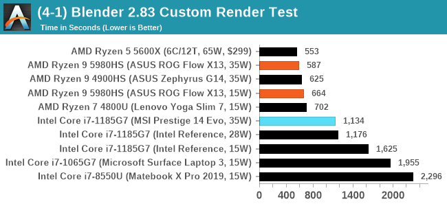
Intel loses out here due to core count, but AMD shows a small but not inconsequential uplift in performance generation-on-generation.
Corona 1.3: Link
Corona is billed as a popular high-performance photorealistic rendering engine for 3ds Max, with development for Cinema 4D support as well. In order to promote the software, the developers produced a downloadable benchmark on the 1.3 version of the software, with a ray-traced scene involving a military vehicle and a lot of foliage. The software does multiple passes, calculating the scene, geometry, preconditioning and rendering, with performance measured in the time to finish the benchmark (the official metric used on their website) or in rays per second (the metric we use to offer a more linear scale).

The standard benchmark provided by Corona is interface driven: the scene is calculated and displayed in front of the user, with the ability to upload the result to their online database. We got in contact with the developers, who provided us with a non-interface version that allowed for command-line entry and retrieval of the results very easily. We loop around the benchmark five times, waiting 60 seconds between each, and taking an overall average. The time to run this benchmark can be around 10 minutes on a Core i9, up to over an hour on a quad-core 2014 AMD processor or dual-core Pentium.
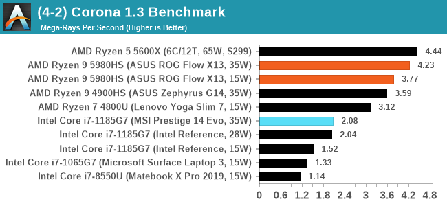
Corona shows a big uplift for Cezanne compared to Renoir.
Crysis CPU-Only Gameplay
One of the most oft used memes in computer gaming is ‘Can It Run Crysis?’. The original 2007 game, built in the Crytek engine by Crytek, was heralded as a computationally complex title for the hardware at the time and several years after, suggesting that a user needed graphics hardware from the future in order to run it. Fast forward over a decade, and the game runs fairly easily on modern GPUs.
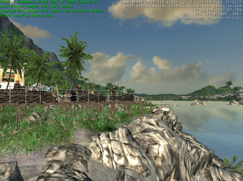
But can we also apply the same concept to pure CPU rendering? Can a CPU, on its own, render Crysis? Since 64 core processors entered the market, one can dream. So we built a benchmark to see whether the hardware can.
For this test, we’re running Crysis’ own GPU benchmark, but in CPU render mode.
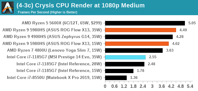
At these resolutions we're seeing a small uplift for Cezanne. We spotted a performance issue when running our 320x200 test where Cezanne scores relatively low (20 FPS vs Renoir at 30 FPS), and so we're investigating that performance issue.
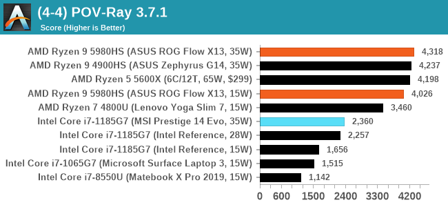
POV-Ray 3.7.1: Link
A long time benchmark staple, POV-Ray is another rendering program that is well known to load up every single thread in a system, regardless of cache and memory levels. After a long period of POV-Ray 3.7 being the latest official release, when AMD launched Ryzen the POV-Ray codebase suddenly saw a range of activity from both AMD and Intel, knowing that the software (with the built-in benchmark) would be an optimization tool for the hardware.
We had to stick a flag in the sand when it came to selecting the version that was fair to both AMD and Intel, and still relevant to end-users. Version 3.7.1 fixes a significant bug in the early 2017 code that was advised against in both Intel and AMD manuals regarding to write-after-read, leading to a nice performance boost.

The benchmark can take over 20 minutes on a slow system with few cores, or around a minute or two on a fast system, or seconds with a dual high-core count EPYC. Because POV-Ray draws a large amount of power and current, it is important to make sure the cooling is sufficient here and the system stays in its high-power state. Using a motherboard with a poor power-delivery and low airflow could create an issue that won’t be obvious in some CPU positioning if the power limit only causes a 100 MHz drop as it changes P-states.
V-Ray: Link
We have a couple of renderers and ray tracers in our suite already, however V-Ray’s benchmark came through for a requested benchmark enough for us to roll it into our suite. Built by ChaosGroup, V-Ray is a 3D rendering package compatible with a number of popular commercial imaging applications, such as 3ds Max, Maya, Undreal, Cinema 4D, and Blender.
We run the standard standalone benchmark application, but in an automated fashion to pull out the result in the form of kilosamples/second. We run the test six times and take an average of the valid results.
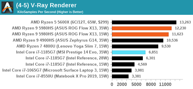
Another good bump in performance here for Cezanne.
Cinebench R20: Link
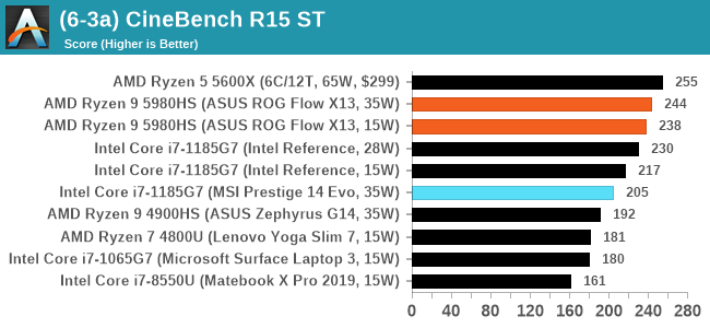
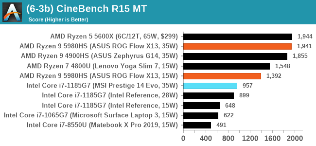
Another common stable of a benchmark suite is Cinebench. Based on Cinema4D, Cinebench is a purpose built benchmark machine that renders a scene with both single and multi-threaded options. The scene is identical in both cases. The R20 version means that it targets Cinema 4D R20, a slightly older version of the software which is currently on version R21. Cinebench R20 was launched given that the R15 version had been out a long time, and despite the difference between the benchmark and the latest version of the software on which it is based, Cinebench results are often quoted a lot in marketing materials.
Results for Cinebench R20 are not comparable to R15 or older, because both the scene being used is different, but also the updates in the code bath. The results are output as a score from the software, which is directly proportional to the time taken. Using the benchmark flags for single CPU and multi-CPU workloads, we run the software from the command line which opens the test, runs it, and dumps the result into the console which is redirected to a text file. The test is repeated for a minimum of 10 minutes for both ST and MT, and then the runs averaged.
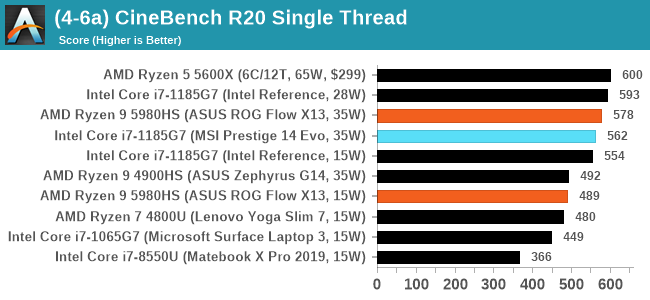
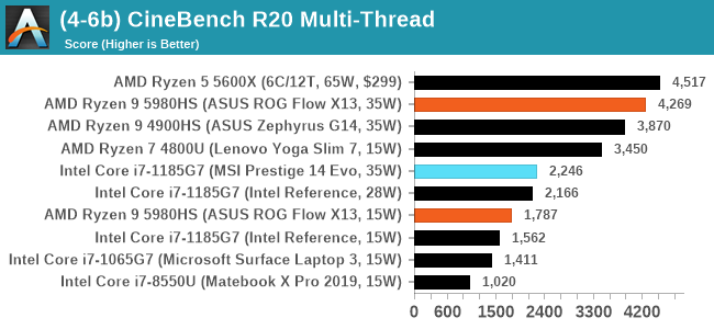
We didn't quite hit AMD's promoted performance of 600 pts here in single thread, and Intel's Tiger Lake is not far behind. In fact, our MSI Prestige 14 Evo, despite being listed as a 35W sustained processor, doesn't seem to hit the same single-core power levels that our reference design did, and as a result Intel's reference design is actually beating both MSI and ASUS in single thread. This disappears in multi-thread, but it's important to note that different laptops will have different single core power modes.
One of the interesting elements on modern processors is encoding performance. This covers two main areas: encryption/decryption for secure data transfer, and video transcoding from one video format to another.
In the encrypt/decrypt scenario, how data is transferred and by what mechanism is pertinent to on-the-fly encryption of sensitive data - a process by which more modern devices are leaning to for software security.
Video transcoding as a tool to adjust the quality, file size and resolution of a video file has boomed in recent years, such as providing the optimum video for devices before consumption, or for game streamers who are wanting to upload the output from their video camera in real-time. As we move into live 3D video, this task will only get more strenuous, and it turns out that the performance of certain algorithms is a function of the input/output of the content.
HandBrake 1.32: Link
Video transcoding (both encode and decode) is a hot topic in performance metrics as more and more content is being created. First consideration is the standard in which the video is encoded, which can be lossless or lossy, trade performance for file-size, trade quality for file-size, or all of the above can increase encoding rates to help accelerate decoding rates. Alongside Google's favorite codecs, VP9 and AV1, there are others that are prominent: H264, the older codec, is practically everywhere and is designed to be optimized for 1080p video, and HEVC (or H.265) that is aimed to provide the same quality as H264 but at a lower file-size (or better quality for the same size). HEVC is important as 4K is streamed over the air, meaning less bits need to be transferred for the same quality content. There are other codecs coming to market designed for specific use cases all the time.
Handbrake is a favored tool for transcoding, with the later versions using copious amounts of newer APIs to take advantage of co-processors, like GPUs. It is available on Windows via an interface or can be accessed through the command-line, with the latter making our testing easier, with a redirection operator for the console output.
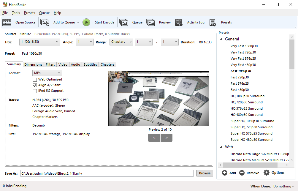
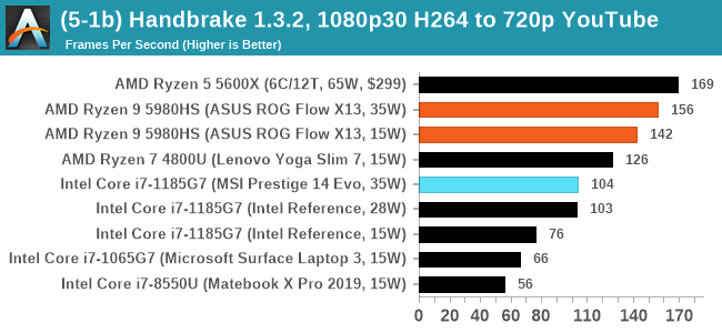
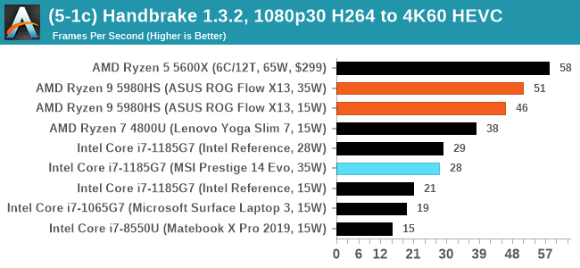
We take the compiled version of this 16-minute YouTube video about Russian CPUs at 1080p30 h264 and convert into three different files: (1) 480p30 ‘Discord’, (2) 720p30 ‘YouTube’, and (3) 4K60 HEVC.
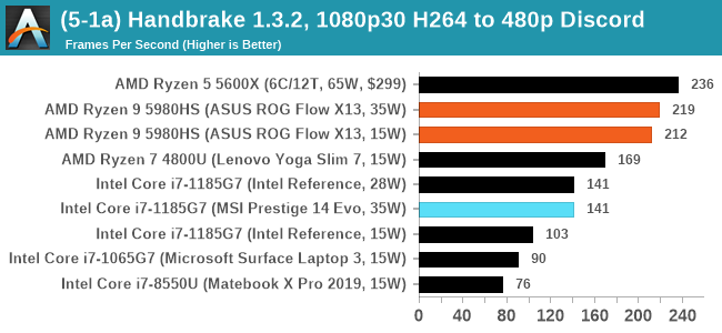
Threads wins, although the +30W difference to the desktop processor with two fewer cores can't be overhauled. Almost though.
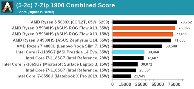
7-Zip 1900: Link
The first compression benchmark tool we use is the open-source 7-zip, which typically offers good scaling across multiple cores. 7-zip is the compression tool most cited by readers as one they would rather see benchmarks on, and the program includes a built-in benchmark tool for both compression and decompression.
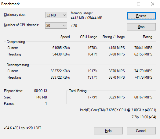
The tool can either be run from inside the software or through the command line. We take the latter route as it is easier to automate, obtain results, and put through our process. The command line flags available offer an option for repeated runs, and the output provides the average automatically through the console. We direct this output into a text file and regex the required values for compression, decompression, and a combined score.
AES Encoding
Algorithms using AES coding have spread far and wide as a ubiquitous tool for encryption. Again, this is another CPU limited test, and modern CPUs have special AES pathways to accelerate their performance. We often see scaling in both frequency and cores with this benchmark. We use the latest version of TrueCrypt and run its benchmark mode over 1GB of in-DRAM data. Results shown are the GB/s average of encryption and decryption.
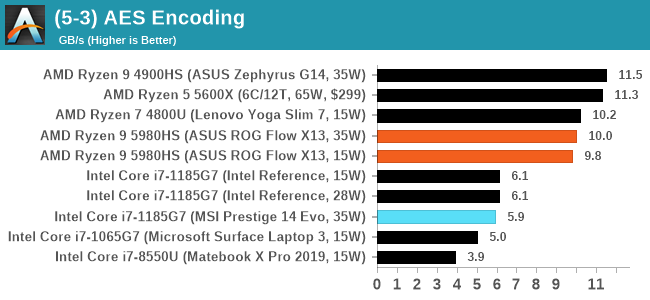
For our AES test here we actually had a small regression in performance. This could mean that there is additional performance hits to accessing the AES unit this time around, or the lower latency DDR4 of the Zephyrus is beating out the LPDDR4 on our Flow X13.
WinRAR 5.90: Link
For the 2020 test suite, we move to the latest version of WinRAR in our compression test. WinRAR in some quarters is more user friendly that 7-Zip, hence its inclusion. Rather than use a benchmark mode as we did with 7-Zip, here we take a set of files representative of a generic stack
- 33 video files , each 30 seconds, in 1.37 GB,
- 2834 smaller website files in 370 folders in 150 MB,
- 100 Beat Saber music tracks and input files, for 451 MB
This is a mixture of compressible and incompressible formats. The results shown are the time taken to encode the file. Due to DRAM caching, we run the test for 20 minutes times and take the average of the last five runs when the benchmark is in a steady state.
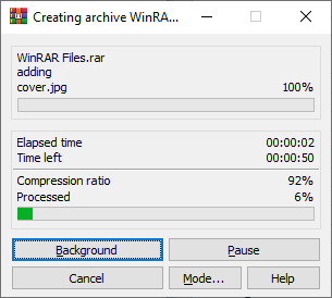
For automation, we use AHK’s internal timing tools from initiating the workload until the window closes signifying the end. This means the results are contained within AHK, with an average of the last 5 results being easy enough to calculate.
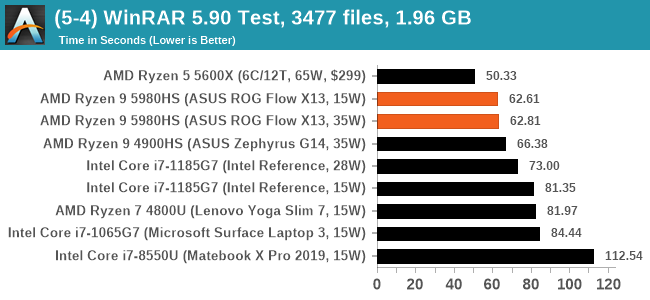
Another small performance uplift for WinRAR.
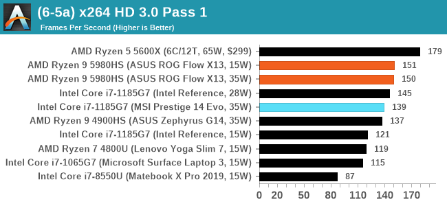
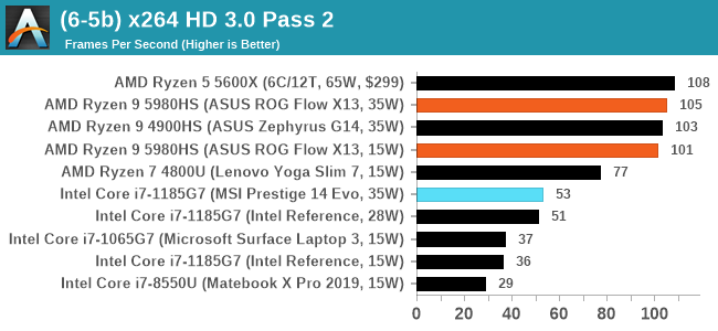
In order to gather data to compare with older benchmarks, we are still keeping a number of tests under our ‘legacy’ section. This includes all the former major versions of CineBench (R15, R11.5, R10) as well as x264 HD 3.0 and the first very naïve version of 3DPM v2.1. We won’t be transferring the data over from the old testing into Bench, otherwise it would be populated with 200 CPUs with only one data point, so it will fill up as we test more CPUs like the others.
The other section here is our web tests.
Web Tests: Kraken, Octane, and Speedometer
Benchmarking using web tools is always a bit difficult. Browsers change almost daily, and the way the web is used changes even quicker. While there is some scope for advanced computational based benchmarks, most users care about responsiveness, which requires a strong back-end to work quickly to provide on the front-end. The benchmarks we chose for our web tests are essentially industry standards – at least once upon a time.
It should be noted that for each test, the browser is closed and re-opened a new with a fresh cache. We use a fixed Chromium version for our tests with the update capabilities removed to ensure consistency.
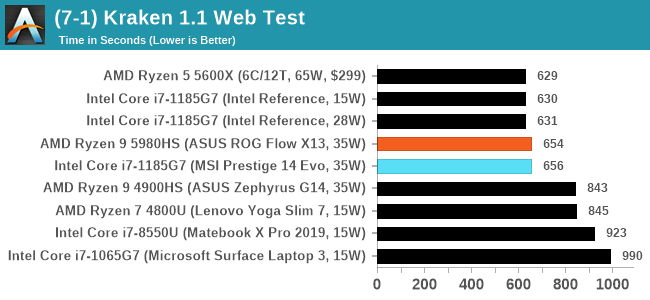
Mozilla Kraken 1.1
Kraken is a 2010 benchmark from Mozilla and does a series of JavaScript tests. These tests are a little more involved than previous tests, looking at artificial intelligence, audio manipulation, image manipulation, json parsing, and cryptographic functions. The benchmark starts with an initial download of data for the audio and imaging, and then runs through 10 times giving a timed result.
We loop through the 10-run test four times (so that’s a total of 40 runs), and average the four end-results. The result is given as time to complete the test, and we’re reaching a slow asymptotic limit with regards the highest IPC processors.
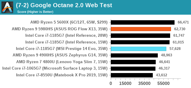
Google Octane 2.0
Our second test is also JavaScript based, but uses a lot more variation of newer JS techniques, such as object-oriented programming, kernel simulation, object creation/destruction, garbage collection, array manipulations, compiler latency and code execution.
Octane was developed after the discontinuation of other tests, with the goal of being more web-like than previous tests. It has been a popular benchmark, making it an obvious target for optimizations in the JavaScript engines. Ultimately it was retired in early 2017 due to this, although it is still widely used as a tool to determine general CPU performance in a number of web tasks.
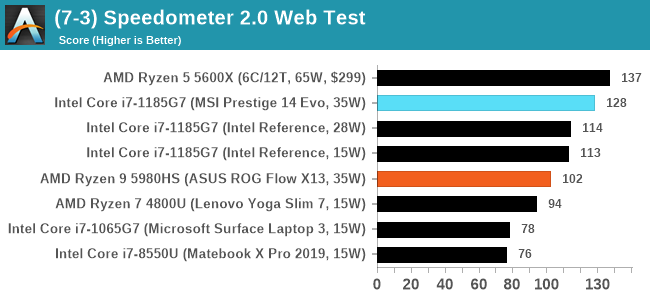
Speedometer 2: JavaScript Frameworks
Our newest web test is Speedometer 2, which is a test over a series of JavaScript frameworks to do three simple things: built a list, enable each item in the list, and remove the list. All the frameworks implement the same visual cues, but obviously apply them from different coding angles.
Our test goes through the list of frameworks, and produces a final score indicative of ‘rpm’, one of the benchmarks internal metrics.
We repeat over the benchmark for a dozen loops, taking the average of the last five.
Most of the people in our industry have a love/hate relationship when it comes to synthetic tests. On the one hand, they’re often good for quick summaries of performance and are easy to use, but most of the time the tests aren’t related to any real software. Synthetic tests are often very good at burrowing down to a specific set of instructions and maximizing the performance out of those. Due to requests from a number of our readers, we have the following synthetic tests.
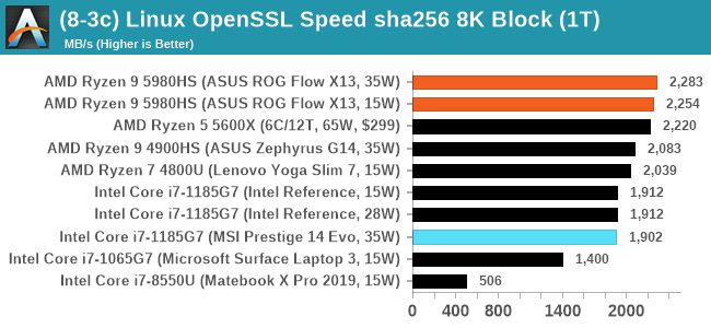
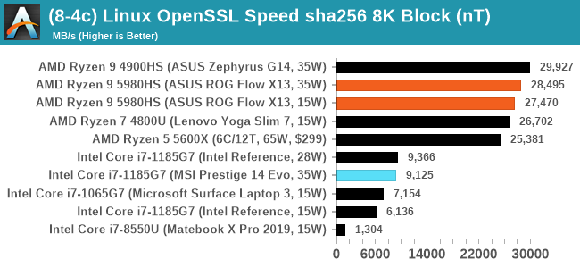
Linux OpenSSL Speed: SHA256
One of our readers reached out in early 2020 and stated that he was interested in looking at OpenSSL hashing rates in Linux. Luckily OpenSSL in Linux has a function called ‘speed’ that allows the user to determine how fast the system is for any given hashing algorithm, as well as signing and verifying messages.
OpenSSL offers a lot of algorithms to choose from, and based on a quick Twitter poll, we narrowed it down to the following:
- rsa2048 sign and rsa2048 verify
- sha256 at 8K block size
- md5 at 8K block size
For each of these tests, we run them in single thread and multithreaded mode. All the graphs are in our benchmark database, Bench, and we use the sha256 results in published reviews.
GeekBench 5: Link
As a common tool for cross-platform testing between mobile, PC, and Mac, GeekBench is an ultimate exercise in synthetic testing across a range of algorithms looking for peak throughput. Tests include encryption, compression, fast Fourier transform, memory operations, n-body physics, matrix operations, histogram manipulation, and HTML parsing.
Unfortunately we are not going to include the Intel GB5 results in this review, although you can find them inside our benchmark database. The reason behind this is down to AVX512 acceleration of GB5's AES test - this causes a substantial performance difference in single threaded workloads that thus sub-test completely skews any of Intel's results to the point of literal absurdity. AES is not that important of a real-world workload, so the fact that it obscures the rest of GB5's subtests makes overall score comparisons to Intel CPUs with AVX512 installed irrelevant to draw any conclusions. This is also important for future comparisons of Intel CPUs, such as Rocket Lake, which will have AVX512 installed. Users should ask to see the sub-test scores, or a version of GB5 where the AES test is removed.
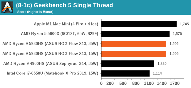
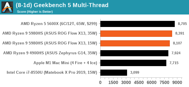
To clarify the point on AES. The Core i9-10900K scores 1878 in the AES test, while 1185G7 scores 4149. While we're not necessarily against the use of accelerators especially given that the future is going to be based on how many and how efficient these accelerators work (we can argue whether AVX-512 is efficient compared to dedicated silicon), the issue stems from a combi-test like GeekBench in which it condenses several different (around 20) tests into a single number from which conclusions are meant to be drawn. If one test gets accelerated enough to skew the end result, then rather than being a representation of a set of tests, that one single test becomes the conclusion at the behest of the others, and it's at that point the test should be removed and put on its own. GeekBench 4 had memory tests that were removed for Geekbench 5 for similar reasons, and should there be a sixth GeekBench iteraction, our recommendation is that the cryptography is removed for similar reasons. There are 100s of cryptography algorithms to optimize for, but in the event where a popular tests focuses on a single algorithm, that then becomes an optimization target and becomes meaningless when the broader ecosystem overwhelmingly uses other cryptography algorithms.
SPEC2017 and SPEC2006 is a series of standardized tests used to probe the overall performance between different systems, different architectures, different microarchitectures, and setups. The code has to be compiled, and then the results can be submitted to an online database for comparison. It covers a range of integer and floating point workloads, and can be very optimized for each CPU, so it is important to check how the benchmarks are being compiled and run.
We run the tests in a harness built through Windows Subsystem for Linux, developed by our own Andrei Frumusanu. WSL has some odd quirks, with one test not running due to a WSL fixed stack size, but for like-for-like testing is good enough. SPEC2006 is deprecated in favor of 2017, but remains an interesting comparison point in our data. Because our scores aren’t official submissions, as per SPEC guidelines we have to declare them as internal estimates from our part.
For compilers, we use LLVM both for C/C++ and Fortan tests, and for Fortran we’re using the Flang compiler. The rationale of using LLVM over GCC is better cross-platform comparisons to platforms that have only have LLVM support and future articles where we’ll investigate this aspect more. We’re not considering closed-sourced compilers such as MSVC or ICC.
clang version 10
clang version 7.0.1 (ssh://git@github.com/flang-compiler/flang-driver.git
24bd54da5c41af04838bbe7b68f830840d47fc03)
-Ofast -fomit-frame-pointer
-march=x86-64
-mtune=core-avx2
-mfma -mavx -mavx2
Our compiler flags are straightforward, with basic –Ofast and relevant ISA switches to allow for AVX2 instructions. We decided to build our SPEC binaries on AVX2, which puts a limit on Haswell as how old we can go before the testing will fall over. This also means we don’t have AVX512 binaries, primarily because in order to get the best performance, the AVX-512 intrinsic should be packed by a proper expert, as with our AVX-512 benchmark. All of the major vendors, AMD, Intel, and Arm, all support the way in which we are testing SPEC.
To note, the requirements for the SPEC licence state that any benchmark results from SPEC have to be labelled ‘estimated’ until they are verified on the SPEC website as a meaningful representation of the expected performance. This is most often done by the big companies and OEMs to showcase performance to customers, however is quite over the top for what we do as reviewers.
For each of the SPEC targets we are doing, SPEC2006 rate-1, SPEC2017 speed-1, and SPEC2017 speed-N, rather than publish all the separate test data in our reviews, we are going to condense it down into a few interesting data points. The full per-test values are in our benchmark database.
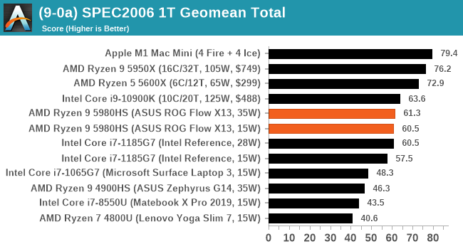
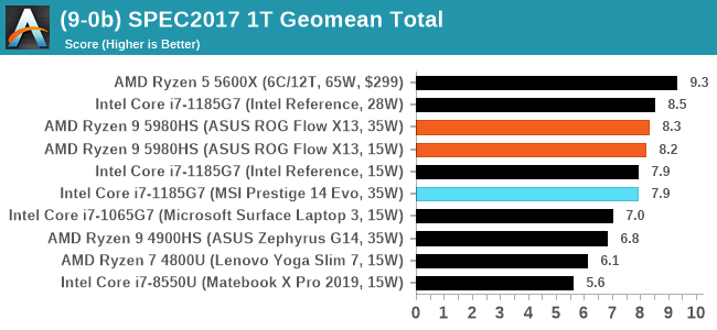
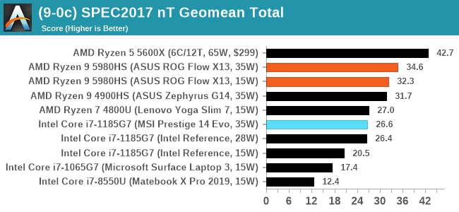
[words]
Testing our Cezanne sample for integrated graphics is a double-edged sword – AMD fully expects this CPU to be paired with a discrete solution in almost all notebook environments, whereas mini-PC designs might be a mix of integrated and discrete. The integrated graphics on this silicon is more geared towards the U-series processors at 15 W, and so that is where the optimizations lie. We encountered a similar environment when we tested Renoir at 35 W last year as well.
In order to enable the integrated graphics on our ASUS ROG Flex X13 system, we disable the GTX 1650 through the device manager. This forces the system to run on the Vega 8 graphics inside, which for this processor runs at 2100 MHz, a +350 MHz jump from the previous generation based on the improved power management and minor manufacturing improvements. We did the same to the other systems in our test suite.
Integrated graphics over the years has been built up from something barely useable in a 2D desktop environment to hardware that can competitively run the most popular eSports titles at good resolutions, medium settings, at playable framerates. In our recent review of AMD’s Ryzen 4000G Desktop APUs, we noted that these were the best desktop APUs that money could buy, held back at this point mostly by the memory bandwidth, but still enabling some good performance. Ultimately modern day integrated graphics has cannibalized the sub-$100 GPU market, and these sorts of processors work great in budget builds. There’s still a way to go on performance, and at least mobile processors help in that regard as more systems push to LPDDR4X memory systems that afford better memory bandwidth.
For our integrated graphics testing, we’re using our lowest configuration for our game comparisons. This typically means the lowest resolution and graphics fidelity settings we can get away with, which to be honest is still a lot better visually than when I used to play Counter Strike 1.5 with my dual core netbook in the late 2000s. From there the goal is to showcase some good graphics performance tied in with CPU performance to see where the limits are – even at 720p on Low settings, some of these processors are still graphics limited.
| Integrated Graphics Benchmark Results | |||||
| AnandTech | Ryzen 9 5980HS |
Ryzen 9 4900HS |
Ryzen 7 4800U |
Core i7 1185G7 |
|
| Power Mode | 35 W | 35 W | 15 W | 28-35 W | |
| Graphics | Vega 8 | Vega 8 | Vega 8 | Iris Xe | |
| Memory | LP4-4267 | D4-3200 | LP4-4267 | LP4-4267 | |
| Frames Per Second Averages | |||||
| Civilization 6 | 480p Min | 101.7 | 98.9 | 68.4 | 66.2 |
| Deus Ex: MD | 600p Min | 80.7 | 76.5 | 61.2 | 69.1 |
| Final Fantasy XV | 720p Med | 31.4 | 31.3 | 29.1 | 36.5 |
| Strange Brigade | 720p Low | 93.2 | 85.2 | 75.7 | 89.3 |
| Borderlands 3 | 360p VLow | 89.8 | 93.6 | - | 64.9 |
| Far Cry 5 | 360p Low | 68.0 | 69.5 | 60.0 | 61.3 |
| GTA 5 | 720p Low | 98.9 | 80.7 | 80.0 | 81.9 |
| Gears Tactics | 720p Low | 86.8 | - | 87.8 | 118.2 |
| 95th Frame Time Percentiles (shown as FPS) | |||||
| Civilization 6 | 480p Min | 69.0 | 67.4 | 45.7 | 43.8 |
| Deus Ex: MD | 600p Min | 45.6 | 57.3 | 38.1 | 44.1 |
| Final Fantasy XV | 720p Med | - | 26.6 | 24.6 | 26.5 |
| Strange Brigade | 768p Min | 84.2 | 77.0 | 68.6 | 73.0 |
| Borderlands 3 | 360p VLow | 63.6 | 73.8 | - | 48.9 |
| Far Cry 5 | 360p Low | 50.3 | 62.3 | 43.8 | 49.8 |
| GTA 5 | 720p Low | 66.8 | 52.8 | 56.0 | 55.7 |
| Gears Tactics | 720p Low | 67.5 | - | 78.3 | 104.5 |
Despite the Ryzen 9 5980HS having LPDDR4X memory and extra frequency, the performance uplift against the Ryzen 9 4900HS is relatively mediocre – a few FPS at best, or losing a few FPS at worst. This is except for GTA, where the uplift is more ~20%, with the Zen 3 cores helping most here. In most tests it’s an easy win against Intel’s top Xe solution, except in Gears Tactics, which sides very heavily with the Intel solution.
With all that being said, as mentioned, the Ryzen 9 parts here are more likely to be paired with discrete graphics solutions. The ASUS ROG Flow X13 we are using today has a GTX 1650, whereas the ASUS Zephyrus G14 with the 4900HS has an RTX 2060. These scenarios are what really dictate the cooling solution in these systems, as well as how they are both used in workloads that requires CPU and GPU performance.
For any users confused as to why we run at these settings; these are our low 'IGP'-class settings in our CPU Gaming test format. The segment above this in our suite is 1440p, which for a lot of these GPUs would put numbers into the low double digits, if not lower, which something we've done in the past to massive complains about why even bothering with such low framerate numbers. The point here is to work from a maximum frame rate, see if the game is even playable to begin with, and then detect where in a game the bottleneck can be; in some of these tests we're still dealing with GPU/DRAM bottlenecks. It provides a starting point for further directions, despite these processors more often being paired with discrete solutions.
The issue with AMD’s notebook strategy through the 2010s was that most users saw the brand as a budget implementation, with low performance and low specifications. Both AMD and its OEM partners were complicit in assisting this projection, using 1366x768 TN screens and slow mechanical hard drives. There were a number of negative feedback loops preventing a nice AMD mobile system from hitting the market, and the only key design wins were from mass corporate sales. With the launch of the first Ryzen Mobile towards the end of the decade, AMD finally had a performance product worthy of attention, and the company has had a steady improvement generation-on-generation, convincing its OEM partners to come along and take advantage of the performance uplift for their customers.
AMD’s historic lows in that 2010 decade were performance, specifications, and battery life. With Ryzen 4000 Mobile, from last generation, AMD had a product that could dispel all those assumptions, and we saw critical acclaim put upon devices like the Lenovo Slim 7 Yoga, and the ASUS Zephyrus G14. From our review of the new generation today, Ryzen 5000 Mobile, the whole strategy that AMD is playing has finally come into focus.
AMD stated that the new generation Ryzen 5000 Mobile processors were in the lab and up-and-running only two months after Ryzen 4000 Mobile launched. AMD made both sets of processors pin-compatible, allowing OEM partners to build designs that could be used for either processor family. The key here that I’ve realized is that AMD’s ultimate goal with these was to build a strong Ryzen 5000 Mobile family, and Ryzen 4000 Mobile was an option for partners to take baby steps, but the main goal was Ryzen 5000, with Zen 3. AMD’s statement of already having over 150+ system designs in the works with Ryzen 5000 Mobile, another +50% over the previous generation, along with this strategy of having a regular predictable cadence of products through re-use of different hardware elements showcases why Ryzen 5000 Mobile is important to the company. With AMD’s recent supply issues as well, we’re of the opinion that AMD has been stockpiling these Ryzen 5000 Mobile processors in order to enable a strong Q1 and Q2 launch of the platform with stock for all OEMs.
What we tested today is one of the AMD flagships for launch, the Ryzen 9 5980HS inside the ASUS ROG Flow X13. This is a sub-16mm ultraportable gaming laptop with a mid-range discrete GPU installed, an impressive 4K 16:10 Pantone certified IPS display, 32GB LPDDR4X memory and a 1 TB NVMe SSD. It also has an executive feel and design, indicating that both AMD and ASUS want to take this platform to its most premium customers. We’re leaving a full review of the laptop itself for a later date, let us focus on the performance of the processor inside.
The jump from Zen 2 to Zen 3 in the mobile space for AMD is more than just putting in the new cores. The cache adjustment from a split 4+4 MB L3 cache to a unified 16 MB L3 cache enables a better effective latency and less reliance on constantly going out to main memory – AMD is also aggressive on the L3 prefetching policies to drive performance. We can see that the single 8-core CCX has low core-to-core communication latency showcasing that enthusiast level workloads will benefit in more ways than one.
AMD is also piling on improvements to help with power, such as enabling different per-core voltage levels and a more efficient memory controller. Per-core voltage control is something that every modern CPU has to have (or at least islands of CPUs) in order to get the best battery performance. AMD is pairing this with its CPPC2 support, and users will benefit from very quick idle-to-turbo performance for immediate responsiveness.
For our benchmark suite, almost all of our benchmarks show an uplift for the new Ryzen 5000 Mobile series, some considerably so: our compile benchmark is +12%, Corona rendering is +18%, Dolphin emulation +17%, NAMD +8%, Blender +6%. To our surprise our SPEC2006 1T benchmark is +32%, accelerated considerably by the 16 MB L3 cache, but also because these CPUs also support a higher instantaneous power turbo modes than the previous generation. This enables some competitive performance numbers against Intel’s Tiger Lake platform in single thread focused tests (AMD wins on multithread quite easily).
All of these core updates, as well as design wins enabling better hardware under the hood, put AMD’s Ryzen 5000 Mobile series in good stead to power a generation of machines especially as more and more of us work from home. When Intel was in a period of high demand through 2018 and 2019, Intel focused on premium solutions to make the most revenue - Intel’s financials last week showed that the company was selling more and more education-focused low-end notebooks and Chromebooks, now that demand had reduced. We can apply something similar to AMD's current situtation - AMD’s silicon is in high demand for 2021, and so AMD’s target this year would appear to be more mid-range, premium commercial, and enthusiast machines. To reaffirm this, AMD has also promised that we will see notebooks this year paired with the most powerful mobile graphics cards, enabling high-performance gamers to move to AMD. No doubt we will have a number pass through our hands through the year, especially as they hit the shelves starting February.
Technology - Latest - Google News
January 26, 2021 at 09:00PM
https://ift.tt/36bCRDS
AMD Ryzen 9 5980HS Cezanne Review: Ryzen 5000 Mobile Tested - AnandTech
Technology - Latest - Google News
https://ift.tt/2AaD5dD
Bagikan Berita Ini


0 Response to "AMD Ryzen 9 5980HS Cezanne Review: Ryzen 5000 Mobile Tested - AnandTech"
Post a Comment