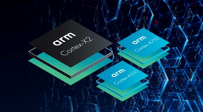
It’s that time of the year again, and after last month’s unveiling of Arm’s newest infrastructure Neoverse V1 and Neoverse N2 CPU IPs, it’s now time to cover the client and mobile side of things. This year, things Arm is shaking things up quite a bit more than usual as we’re seeing new three new generation microarchitectures for mobile and client: The flagship Cortex-X2 core, a new A78 successor in the form of the Cortex-A710, and for the first time in years, a brand-new little core with the new Cortex-A510. The three new CPUs form a new trio of Armv9 compatible designs that aim to mark a larger architectural/ISA shift that comes very seldomly in the industry.
Alongside the new CPU cores, we’re also seeing a new L3 and cluster design with the DSU-110, and Arm is also making a big upgrade in its interconnect IP with the new cache coherent CI-700 mesh network and NI-700 network-on-chip IPs.
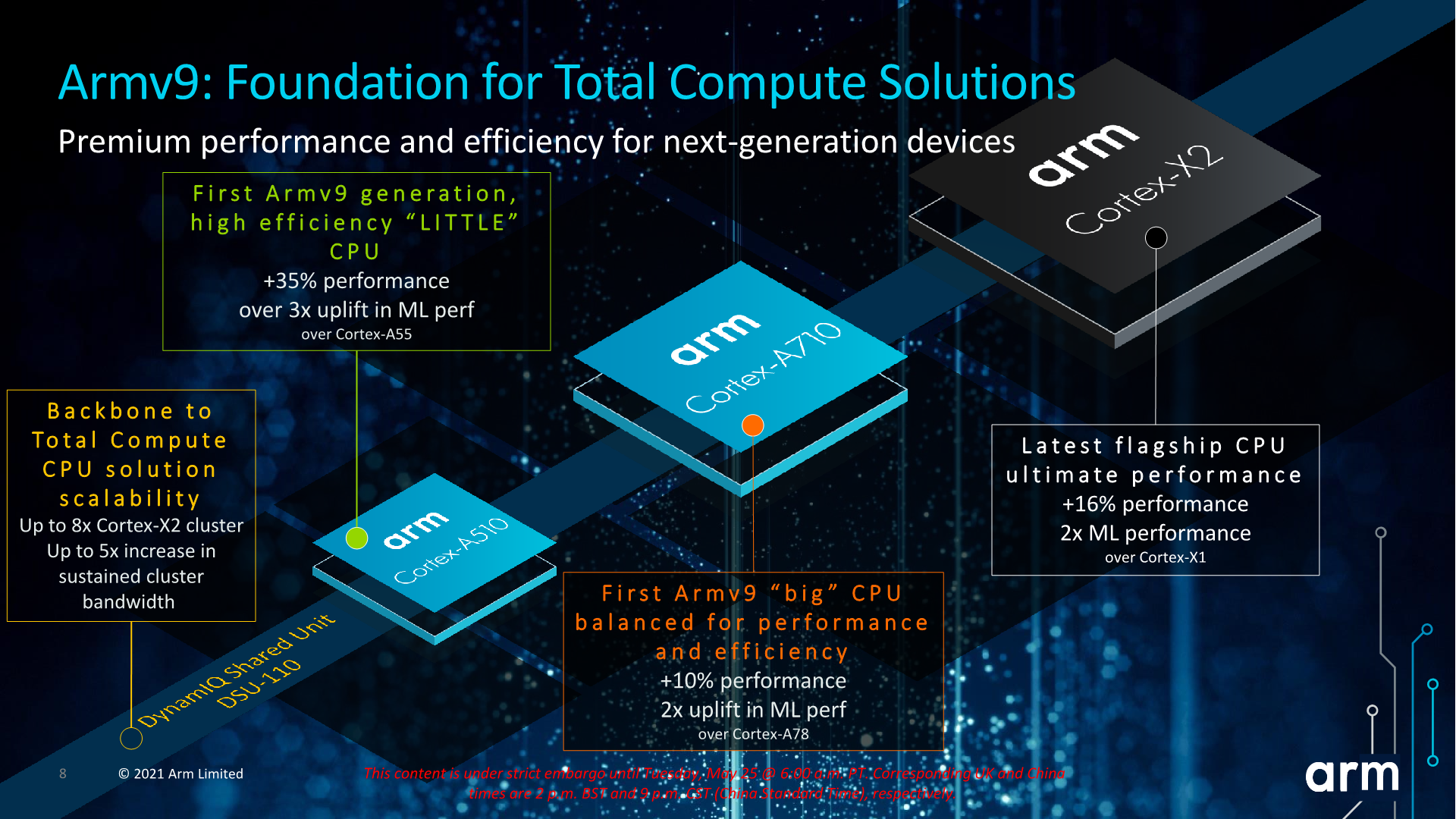
The Cortex-X2, A710 and A510 follow up on last year's X1, A78 and A55. For the new Cortex-X2 and A710 in particular, these are direct microarchitectural successors to their predecessors. These parts, while iterating on generational improvements in IPC and efficiency, also incorporate brand-new architectural features in the form of Armv9 and new extensions such as SVE2.
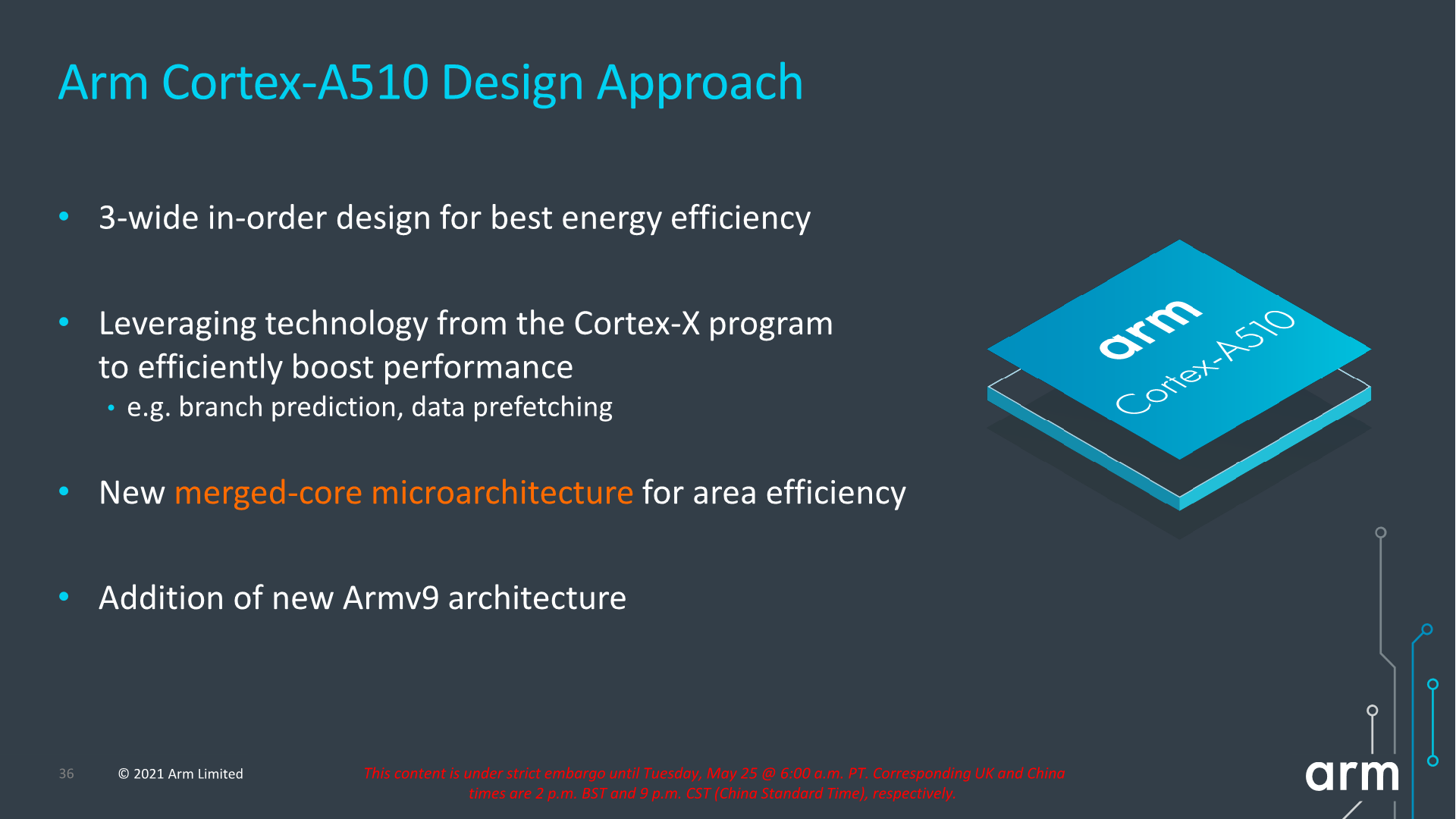
The Cortex-A510, Arm's new little core, is a larger microarchitectural jump, as it represents a new clean-sheet CPU design from Arm’s Cambridge CPU design team. A510 brings large IPC improvements while still having a continued focus on power efficiency, and, perhaps most interestingly, retains its characteristic in-order microarchitectural.
An Armv9 CPU Family – AArch64 only for all practical purposes*
The new CPU family marks one of the largest architectural jumps we’ve had in years, as the company is now baselining all three new CPU IPs on Armv9.0. We've extensively covered the details of the new Arm architecture back in late March. Cornerstone features of the new ISA include the new enrollment of prior optional/missing Armv8.2+ features that weren’t guaranteed in mobile and client designs (mostly due to the older A55 cores), and the introduction of new SVE2 SIMD and vector extensions.
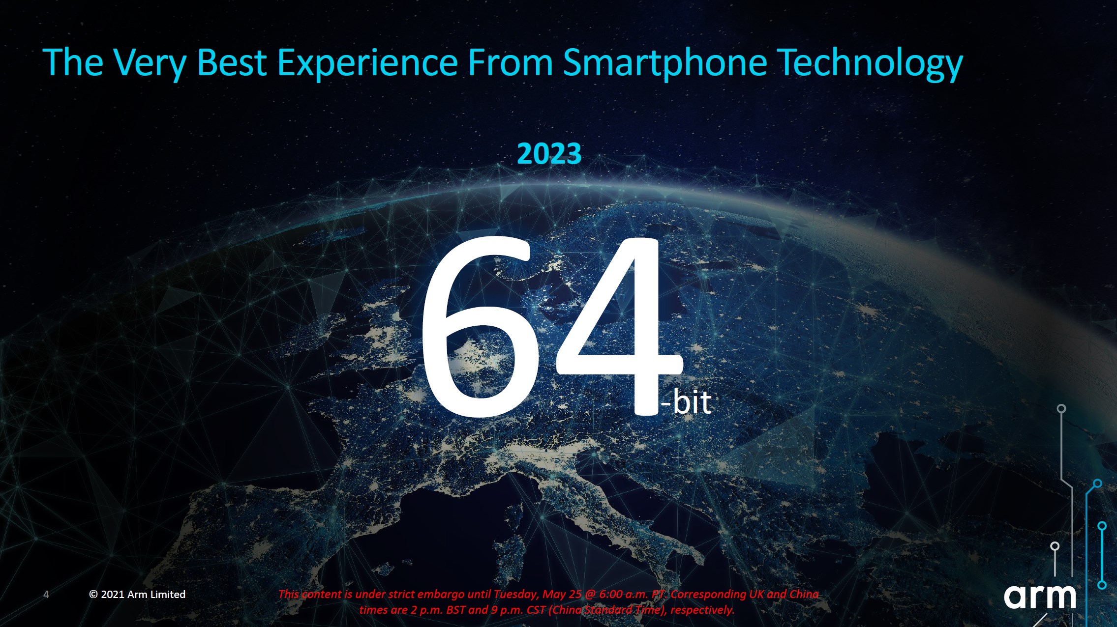
One big change we’ve been expecting for quite some time now is that we’ll be seeing a deprecation of the 32-bit AArch32 execution mode in upcoming Arm Cortex-A mobile cores. The clock has been ticking for 32-bit apps ever since Google’s announced in 2019 that the Google Play store will require for 64-bit app uploads, and the company will stop serving 32-bit applications to 64-bit compatible devices later this summer
While Arm is declaring that shift to happen in 2023, for all intents and purposes it’s already happening next year for most global users. Both the Cortex-X2 flagship core and the Cortex-A510 little cores are AArch64-only microarchitectures that are no longer able to execute AArch32 code.
With that said, sharp readers will note that two out of three CPUs isn't a complete shift, and the reason for that is because the Cortex-A710 actually still supports AArch32. Arm states that the reason for this is primarily to meet the needs of the Chinese mobile market, which lacks the homogeneous ecosystem capabilities of the global Play Store markets, and Chinese vendors and their domestic app market require a little more time to facilitate the shift towards 64-bit only. This means we’ll have an odd scenario next year of having SoCs on which only the middle cores are able to execute 32-bit applications, with those apps being relegated to the middle A710 cores and missing out on the little A510 cores’ power efficiency or the X2 cores’ performance.
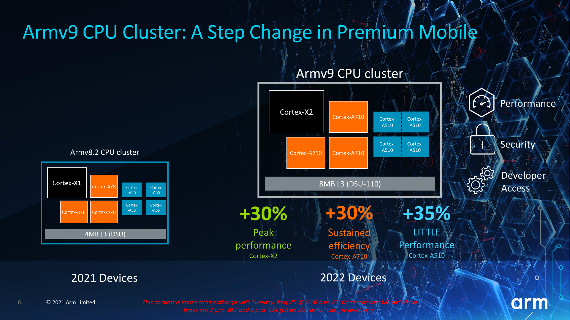
On the big core side, the new Cortex-X2 and Cortex-A710 are successors to the Cortex-X1 and Cortex-A78. Both designs are mostly designed by Arm’s Austin design team, and represent the 4th generation of this microarchitecture family, which had started off with the Cortex-A76 several years ago. These cores should be the last of this microarchitecture family before Arm hands things off to a completely new design with next year’s new Sophia cores.
In terms of design philosophy, the X2 and A710 generally keep the same overarching goals the X1 and A78 had defined: The X-series continues to focus on advancing performance by increasing microarchitectural structures and by Arm being willing to make compromises on power within reasonable limits. Meanwhile the A710 continues to focus on advancing performance and efficiency through smarter design and with a large focus on maximizing the power, performance, and area (PPA) balance of the IP.
One point Arm makes in the above slide is having optimized critical paths and physical design for sustained voltage operations – this is more of a goal the company is striving for in the next generations of “middle” cores rather than something that’s specifically reflected in the Cortex-A710.
This year, we are also finally seeing a new little core. We had covered the Cortex-A55 back in 2017, and since then we haven’t had seen any updates to Arm’s little cores, to the point of it being seen as large weakness of last few generations of mobile SoCs.
The new Cortex-A510 is a clean-sheet design from Arm’s Cambridge design team, leveraging a lot of the technologies that had been employed in the company’s larger cores, but implemented into a new in-order little microarchitecture. Yes – we’re still talking about an in-order core, and Arm still sees this to be the best choice in terms of extracting the best efficiency and “Days of use” of mobile devices.
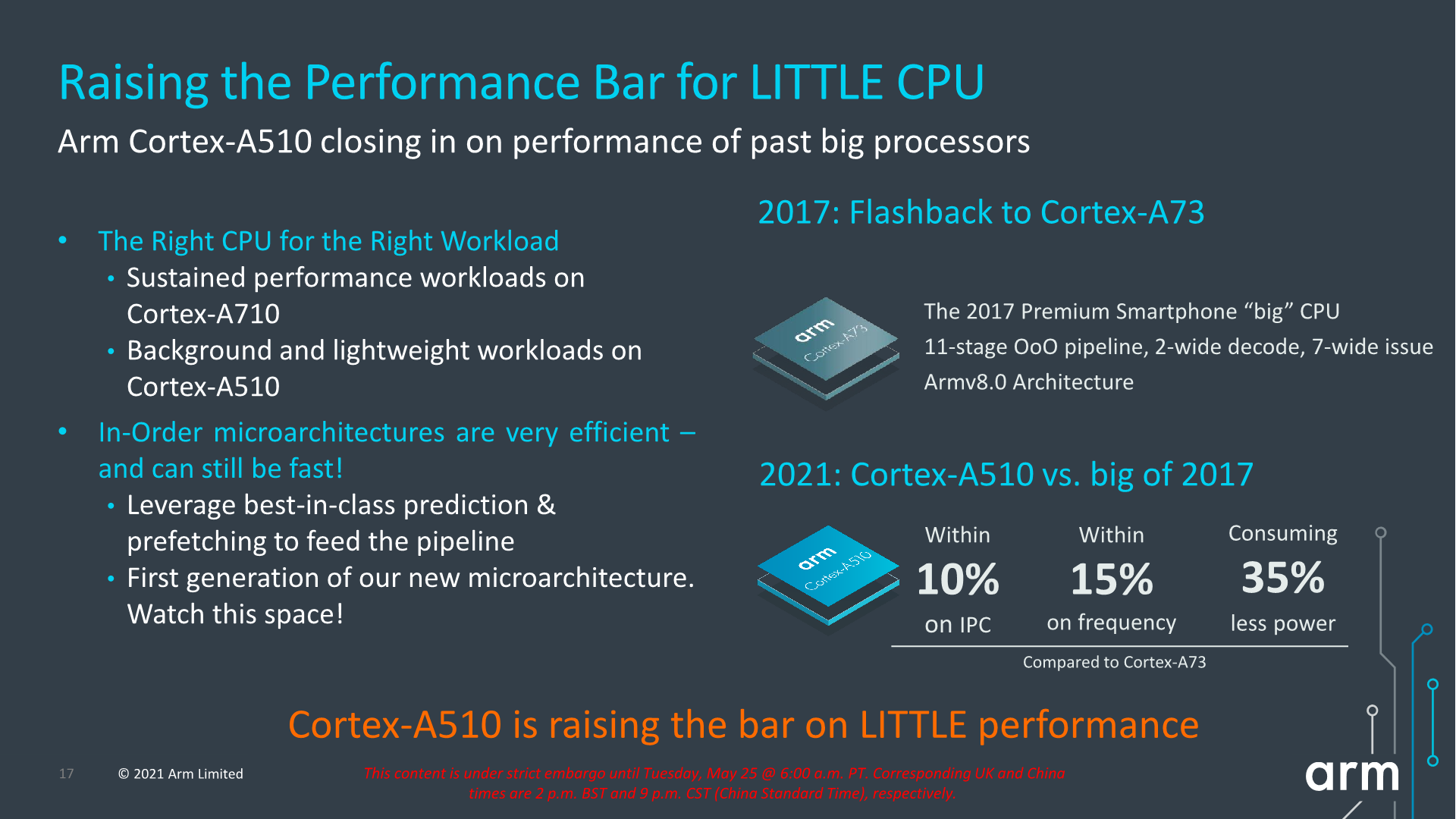
Even though it’s a in-order core, Arm made a comparison that the new design is extremely similar to a flagship core of 2017 – namely the Cortex-A73, achieving very similar IPC and frequency capabilities whilst consuming a lot less power.
The new design also comes with a very interesting shared complex approach and shares the L2 and FP/SIMD pipelines with a second core, a design approach Arm calls “merged core” and undoubtedly will remind readers of AMD’s CMT approach in Bulldozer cores 10 years ago, even though there are quite important differences in the approaches.
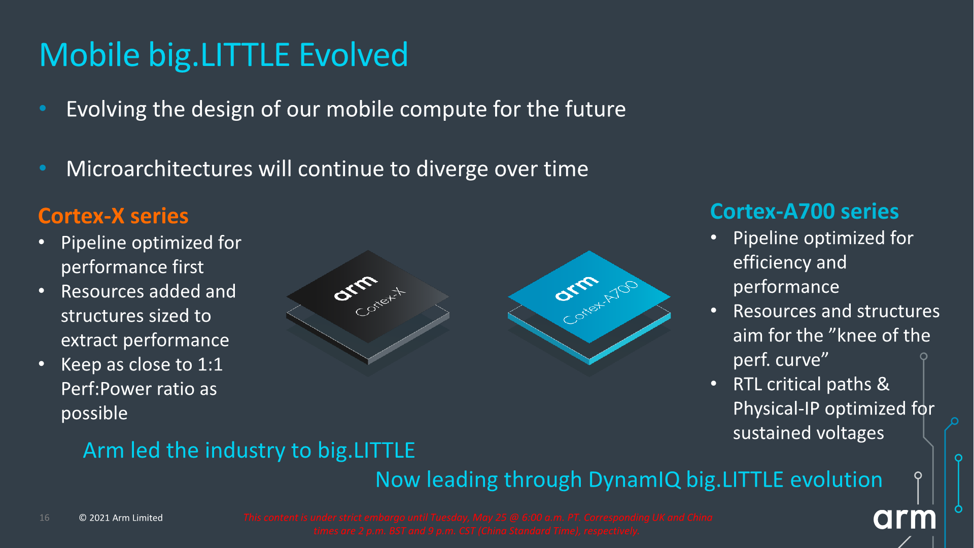
We first start off with the Cortex-X2, successor to last year’s Cortex-X1. The X1 marked the first in a new IP line-up from Arm which diverged its “big” core offering into two different IP lines, with the Cortex-A sibling continuing Arm’s original design philosophy of PPA, while the X-cores are allowed to grow in size and power in order to achieve much higher performance points.
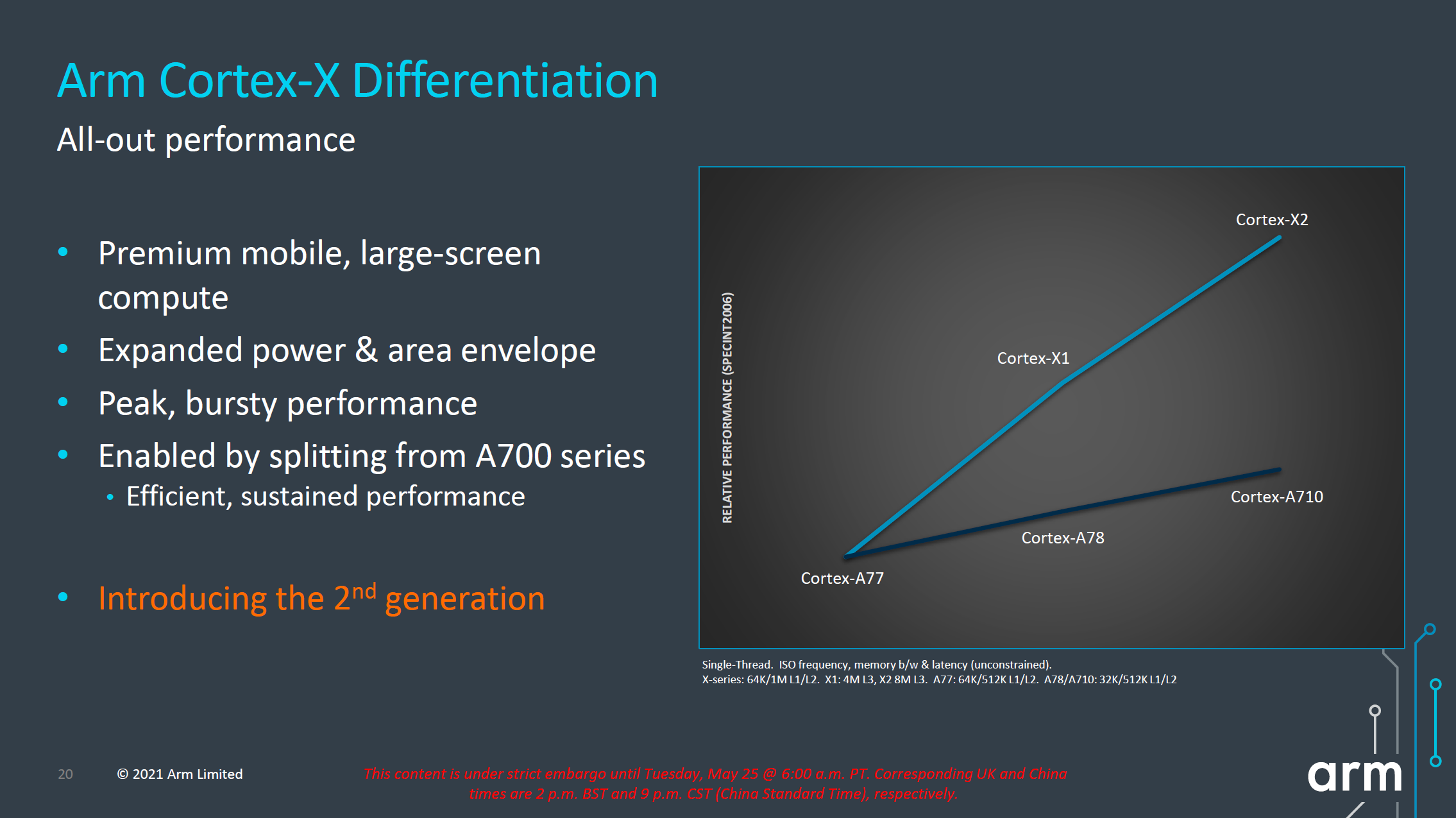
The Cortex-X2 continues this philosophy, and further grows the performance and power gap between it and its “middle” sibling, the Cortex-A710. I also noticed that throughout Arm’s presentation there were a lot more mentions of having the Cortex-X2 being used in larger-screen compute devices and form-factors such as laptops, so it might very well be an indication of the company that some of its customers will be using the X2 more predominantly in such designs for this generation.
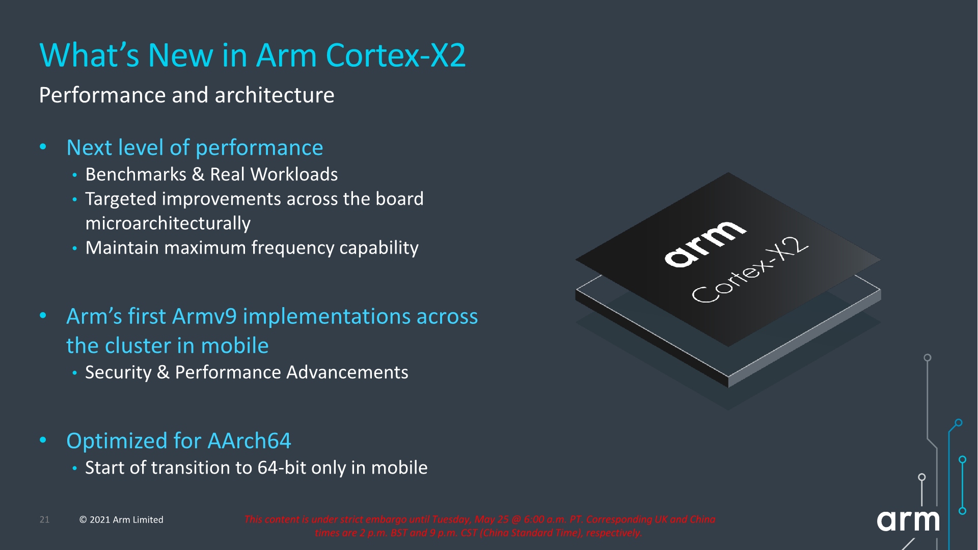
From an architectural standpoint the X2 is naturally different from the X1, thanks in large part to its support for Armv9 and all of the security and related ISA platform advancements that come with the new re-baselining of the architecture.
As noted in the introduction, the Cortex-X2 is also a 64-bit only core which only supports AArch64 execution, even in PL0 user mode applications. From a microarchitectural standpoint this is interesting as it means Arm will have been able to kick out some cruft in the design. However as the design is a continuation of the Austin family of processors, I do wonder if we’ll see more benefits of this deprecation in future “clean-sheet” big cores designs, where AArch64-only was designed from the get-go. This, in fact, is something that's already happening in other members of Arm's CPU cores, as the new little core Cortex-A510 was designed sans-AArch32.
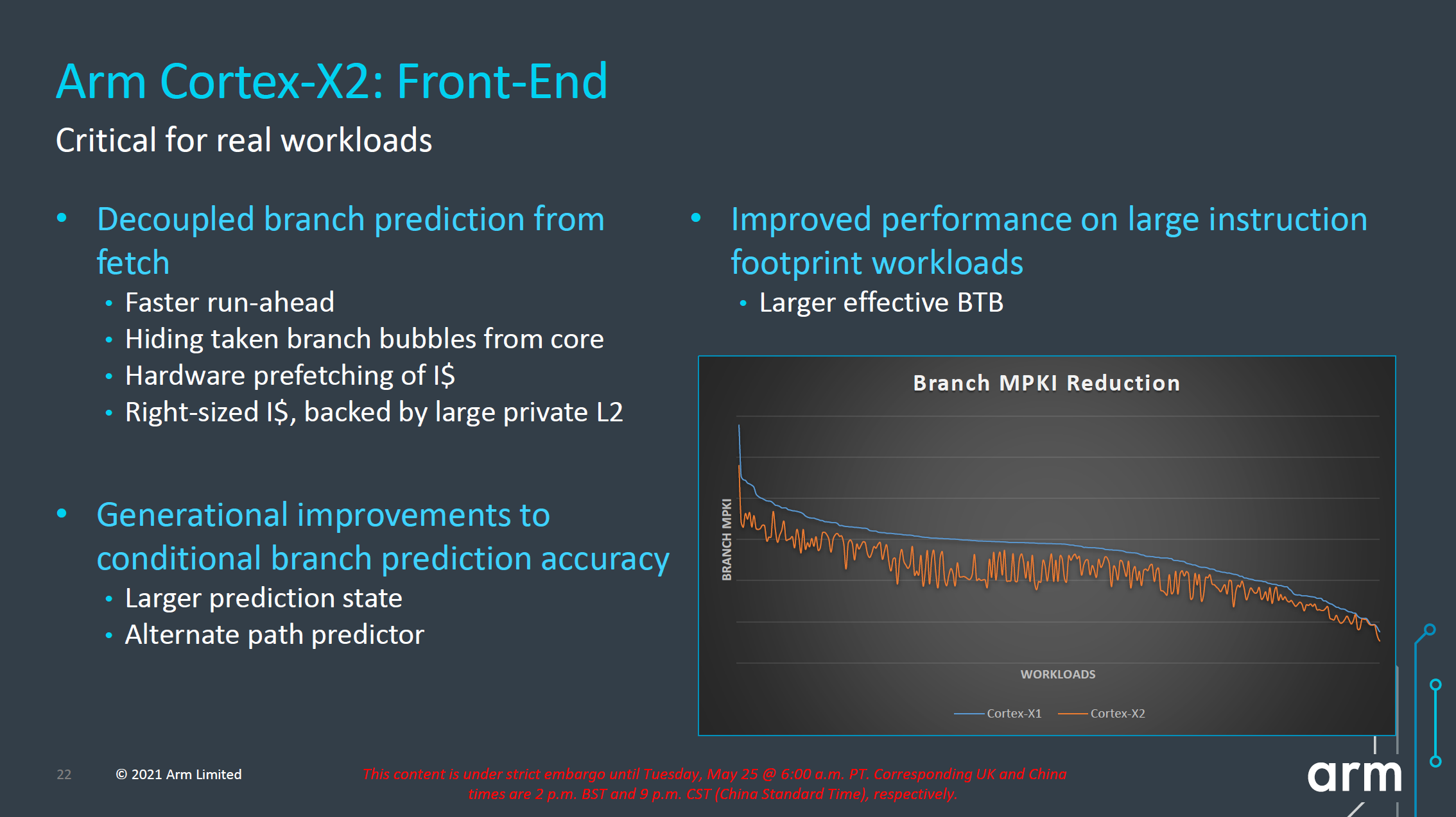
Starting off with the front-end, in general, Arm has continued to try to improve what it considers the most important aspect of the microarchitecture: branch prediction. This includes continuing to run the branch resolution in a decoupled way from the fetch stages in order to being able to have these functional blocks be able to run ahead of the rest of the core in case of mispredicts and minimize branch bubbles. Arm generally doesn’t like to talk too much details about what exactly they’ve changed here in terms of their predictors, but promises a notable improvement in terms of branch prediction accuracy for the new X2 and A710 cores, effectively reducing the MPKI (Misses per kilo instructions) metric for a very wide range of workloads.
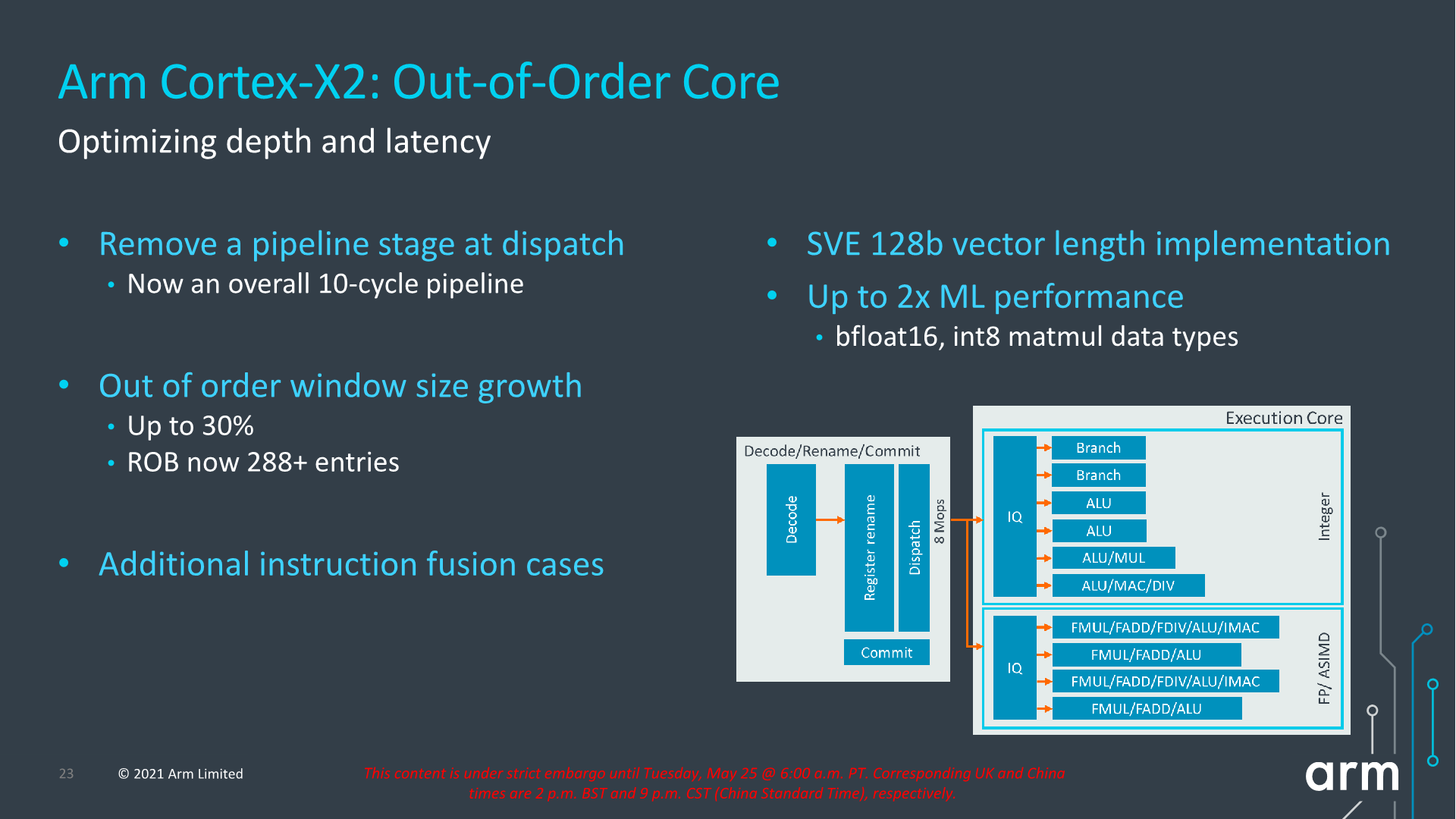
The new core overall reduces its pipeline length from 11 cycles to 10 cycles as Arm has been able to reduce the dispatch stages from 2-cycles to 1-cycle. It’s to be noted that we have to differentiate the pipeline cycles from the mispredict penalties, the latter had already been reduced to 10 cycles in most circumstances in the Cortex-A77 design. Removing a pipeline stage is generally a rather large change, particularly given Arm’s target of maintaining frequency capabilities of the core. This design change did incur some more complex engineering and had area and power costs; but despite that, as Arm explains in, cutting a pipeline stage still offered a larger return-on-investment when it came to the performance benefits, and was thus very much worth it.
The core also increases its out-of-order capabilities, increasing the ROB (reorder buffer) by 30% from 224 entries to 288 entries this generation. The effective figure is actually a little bit higher still, as in cases of compression and instruction bundling there are essentially more than 288 entries being stored. Arm says there’s also more instruction fusion cases being facilitated this generation.
On the back-end of the core, the big new change is on the part of the FP/ASIMD pipelines which are now SVE2-capable. In the mobile space, the SVE vector length will continue to be 128b and essentially the new X2 core features similar throughput characteristics to the X1’s 4x FP/NEON pipelines. The choice of 128b vectors instead of something higher is due to the requirement to have homogenous architectural feature-sets amongst big.LITTLE designs as you cannot mix different vector length microarchitectures in the same SoC in a seamless fashion.
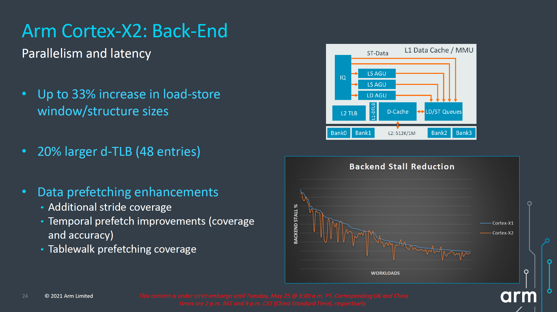
On the back-end, the Cortex-X2 continues to focus on increasing MLP (memory level parallelism) by increasing the load-store windows and structure sizes by 33%. Arm here employs several structures and generally doesn’t go into detail about exactly which queues have been extended, but once we get our hands on X2 systems we’ll be likely be able to measure this. The L1 dTLB has grown from 40 entries to 48 entries, and as with every generation, Arm has also improved their prefetchers, increasing accuracies and coverage.
One prefetcher that surprised us in the Cortex-X1 and A78 earlier this year when we first tested new generation devices was a temporal prefetcher – the first of its kind that we’re aware of in the industry. This is able to latch onto arbitrary repeated memory patterns and recognize new iterations in memory accesses, being able to smartly prefetch the whole pattern up to a certain depth (we estimate a 32-64MB window). Arm states that this coverage is now further increased, as well as the accuracy – though again the details we’ll only able to see once we get our hands on silicon.
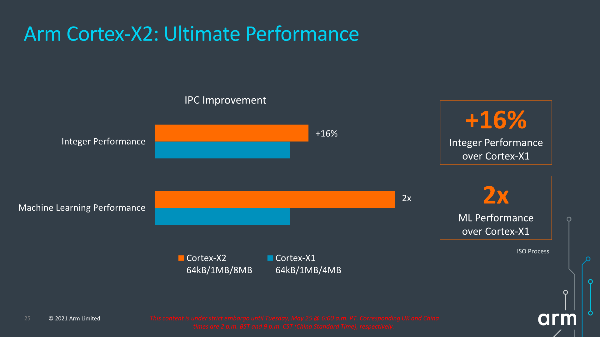
In terms of IPC improvements, this year’s figures are quoted to reach +16% in SPECint2006 at ISO frequency. The issue with this metric (and which applies to all of Arm’s figures today) is that Arm is comparing an 8MB L3 cache design to a 4MB L3 design, so I expect a larger chunk of that +16% figure to be due to the larger cache rather than the core IPC improvements themselves.
For their part, Arm is reiterating that they're expecting 8MB L3 designs for next year’s X2 SoCs – and thus this +16% figure is realistic and is what users should see in actual implementations. But with that said, we had the same discussion last year in regards to Arm expecting 8MB L3 caches for X1 SoCs, which didn't happen for either the Exynos 2100 nor the Snapdragon 888. So we'll just have to wait and see what cache sizes the flagship commercial SoCs end up going with.

In terms of the performance and power curve, the new X2 core extends itself ahead of the X1 curve in both metrics. The +16% performance figure in terms of the peak performance points, though it does come at a cost of higher power consumption.
Generally, this is a bit worrying in context of what we’re seeing in the market right now when it comes to process node choices from vendors. We’ve seen that Samsung’s 5LPE node used by Qualcomm and S.LSI in the Snapdragon 888 and Exynos 2100 has under-delivered in terms of performance and power efficiency, and I generally consider both big cores' power consumption to be at a higher bound limit when it comes to thermals. I expect Qualcomm to stick with Samsung foundry in the next generation, so I am admittedly pessimistic in regards to power improvements in whichever node the next flagship SoCs come in (be it 5LPP or 4LPP). It could well be plausible that we wouldn’t see the full +16% improvement in actual SoCs next year.
While the Cortex-X2 goes for all-out performance while paying the power and area penalties, Arm's Cortex-A710 design goes for a more efficient approach.
First of all, the new product nomenclature now is self-evident in regards to what Arm will be doing going forward- they’re skipping the A79 designation and simply starting fresh with a new three-digit scheme with the A710. Not very important in the grand scheme of things but an interesting marketing tidbit.
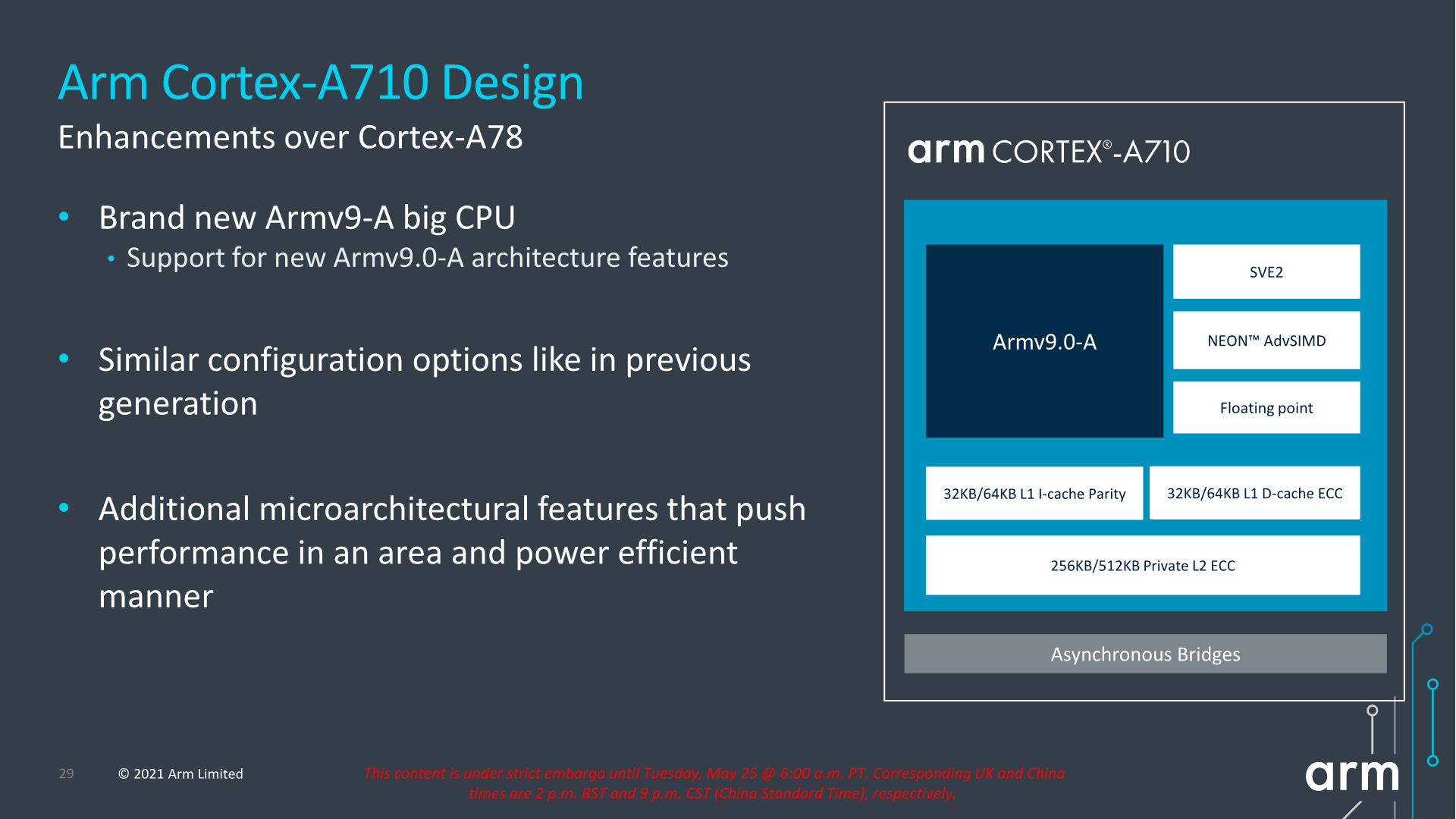
The Cortex-A710, much like the X2, is an Armv9 core with all new features that come with the new architecture version. Unlike the X2, the A710 also supports PL0 AArch32 execution, and as mentioned in the intro, this was mostly a design choice demanded by customers in the Chinese market where the ecosystem is still slightly lagging behind in moving all applications over to AArch64.
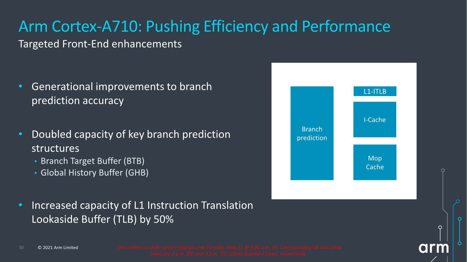
In terms of front-end enhancements, we’re seeing the same branch prediction improvements as on the X2, with larger structures as well as better accuracy. Other structures such as the L1I TLB have also seen an increase from 32 entries to 48 entries. Other front-end structures such as the macro-OP cache remain the same at 1.5K entries (The X2 also remains at 3K entries).
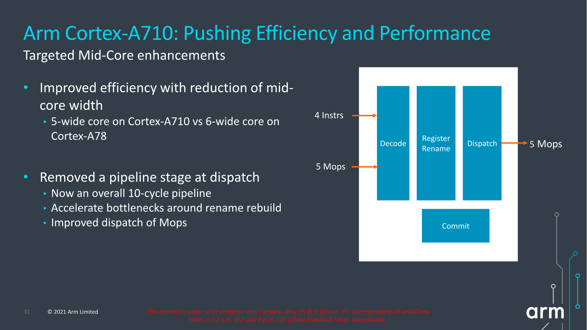
A very interesting choice for the A710 mid-core is that Arm has reduced the macro-OP cache and dispatch stage throughputs from 6-wide to 5-wide. This was mainly a targeted power and efficiency optimization for this generation, as we’re seeing a more important divergence between the Cortex-A and Cortex-X cores in terms of their specializations and targeted use-cases for performance and power.
The dispatch stage also features the same optimizations as on the X2, removing 1 cycle from the pipeline towards an overall 10-cycle pipeline design.
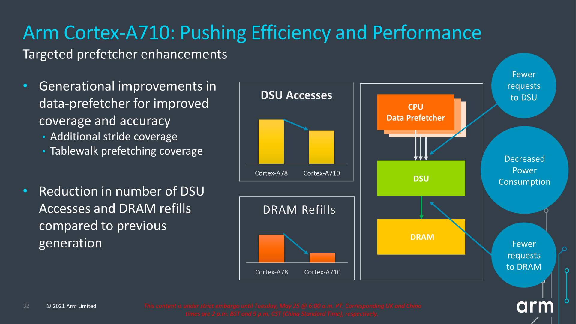
Arm also focuses on core improvements that affect the uncore parts of the system, which take place thanks to the new improvements in the prefetcher designs and how they interact with the new DSU-110 (which we’ll cover later). The new combination of core and DSU are able to reduce access from the core towards the L3 cache, as well as reducing the costly DRAM accesses thanks to the more efficiency prefetchers and larger L3 cache.
In terms of IPC, Arm advertises +10%, but again the issue with this figure here is that we’re comparing an 8MB L3 cache design to a 4MB L3 cache design. While this is a likely comparison for flagship SoCs next year, because the Cortex-A710 is also a core that would be used in mid-range or lower-end SoCs which might use much smaller L3 caches, it’s unlikely we’ll be seeing such IPC improvements in that sector unless the actual SoCs really do also improve their DSU sizes.
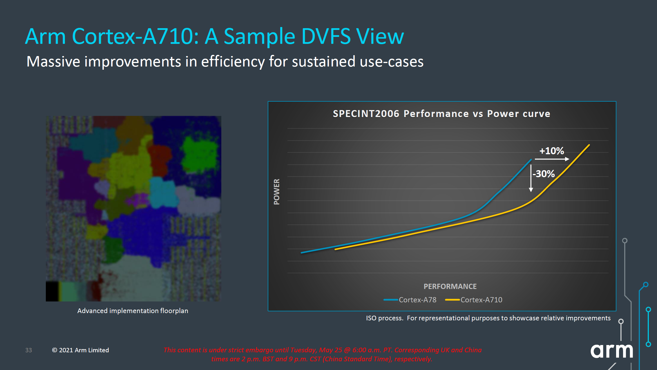
More important than the +10% improvement in performance is that, when backing off slightly in frequency, we can see that the power reduction can be rather large. According to Arm, at iso-performance the A710 consumes up to 30% less power than the Cortex-A78. This is something that would greatly help with sustained performance and power efficiency of more modestly clocked “middle” core implementations of the Cortex-A710.
In general, both the X2 and the A710’s performance and power figures are quite modest, making them the smallest generation-over-generation figures we’ve seen from Arm in quite a few years. Arm explains that due to this generation having made larger architectural changes with the move to Armv9, there has been an impact in regards to the usual efficiency and performance improvements that we’ve seen in prior generations.
Both the X2 and the A710 are also the fourth generation of this Austin microarchitecture family, so we’re hitting a wall of diminishing returns and maturity of the design. A few years ago we were under impression that the Austin family would only go on for three generations before handing things over to a new clean-sheet design from the Sophia team, but that original roadmap has been changed, and now we'll be seeing the new Sophia core with larger leaps in performance being disclosed next year.
Moving on from the larger cores, this year we also have the pleasure to cover Arm’s newest little core, the new Cortex-A510. The new design if a clean-sheet microarchitecture from Arm’s Cambridge team which the engineers had been working on the past 4 years, and marks a quite different approach when it comes to how the little cores are built into the SoC.
First of all, Arm made explicit note of the design’s continued use of an in-order execution flow, mentioning that in their view that this is still the most power-efficient way to design a core for such workloads. This remains a relatively controversial topic and point of discussion when put into context of Apple’s own out-of-order efficiency cores, a topic I’ll return on later.
Secondly, the Cortex-A510 introduces something called a “merged-core” microarchitecture, there’s some very high-level comparisons and similarities to what AMD had done with CMT in their Bulldozer cores a decade ago, but differs quite significantly in some important aspects in terms of the details and design.
Of course, like the X2 and A710, the A510 is an Armv9 design, and all three cores share the same architectural features with each other, allowing them to be integrated together into the same SoC. It’s to be noted that the A510, much like the X2, is a 64-bit only AArch64 core.
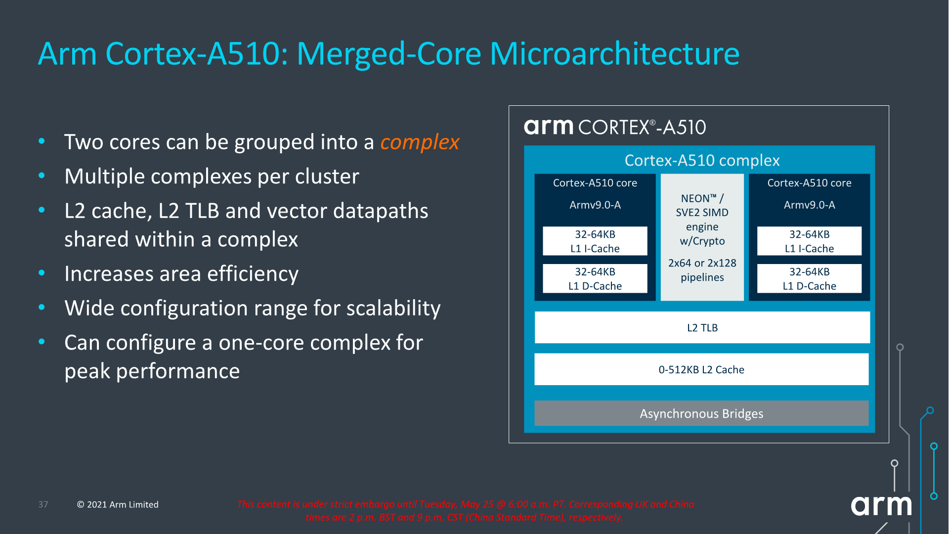
The most interesting aspect of the Cortex-A510 is the new merged-core approach. What Arm is doing here, is creating a new “complex” of up to two core pairs, which share the L2 cache system as well as the FP/NEON/SVE pipelines between them.
At first glance this will sound extremely similar to what AMD had done with Bulldozer and the CMT (Clustered Multithreading) approach, however Arm’s design is much more disaggregated in terms of what the actual cores are sharing. While AMD’s CMT module consisted essentially of a shared front-end between two integer back-ends and a single FP/SIMD back-end, Arm’s “merged cores” are actually full cores with their individual front-ends, mid-core, integer back-ends, and L1 cache hierarchies. The only thing being shared between the “cores” is the actual FP/SIMD back-end, as well as the L2 cache hierarchy.
Furthermore, while in the mobile market we expect vendors to use this new two merged cores per complex approach, it’s actually possible to simply just have a single core per complex. In which case the solo core would essentially have its own dedicated (non-shared) resources, but would be notably less area efficient than the intended merged core approach.
Generally, given the adoption of SVE2 and the relatively larger area footprint that the new execution backend requires, it makes sense to actually share these resources for these tiny new cores. Their typical workloads are also mostly only integer-bound background workloads which put less pressure on such units.
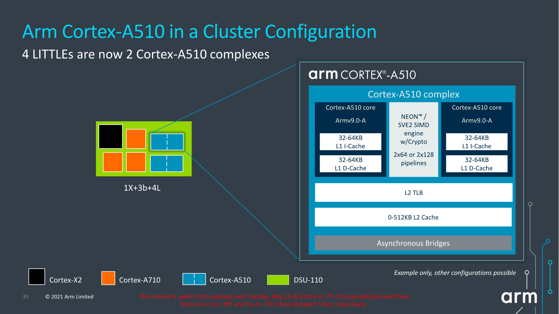
From a higher-level SoC standpoint, nothing really changes when it comes to the core-count, with the details being that we’ll be seeing two pairs or little cores now share a larger L2 cache between each other. This L2 can be configured up to 512KB, but as always, what we’ll actually see in products will very much depend on what vendors will want to implement into their designs. Because the new complex also only takes up a single interface on the DSU, it also opens up the possibility of designs larger than 8 “cores”, something I hope won’t happen, or hopefully only happens through more middle or big cores.
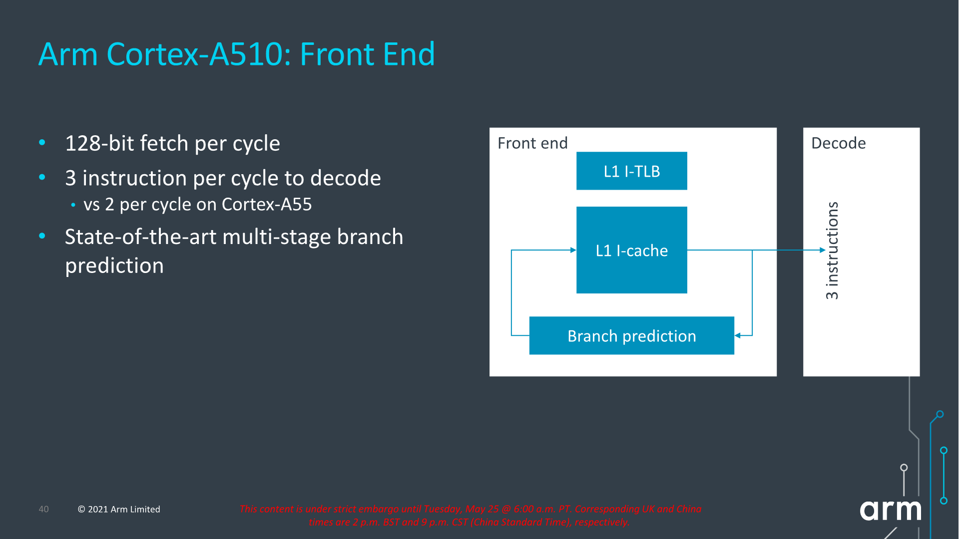
In terms of the front-end of the new A510, we’re seeing a 128-bit fetch pipeline which means it can fetch up to 4 instructions per cycle, giving the front-end a bit of leeway to close branch bubbles. The actual width of the decoder has increased from 2-wide to 3-wide.
In terms of branch prediction, as always Arm doesn’t disclose too many details, however the company did note that it used the same state-of-the-art approaches and techniques it uses on its larger cores. The L1 instruction cache can be either 32 or 64KB.

In terms of the shared vector execution back-end, it’s actually quite interesting here as Arm gives the option of either configuring the complex with smaller 2x64-bit pipelines or with 2x128b pipelines, the latter whose throughput would be 2x that of a Cortex-A55. I’m not too sure what mobile vendors will go with; we always hope for the larger configuration but as always, we’ll have to wait and see what will be employed in the actual products. In both configurations, the vector length is 128b as that’s the requirements for interoperability for the larger core microarchitectures.
Arm states that the shared pipelines are completely transparent to hardware, and that it’s also using fine-grained hardware scheduling. In actual multi-threaded workloads using both cores, the performance impact and deficit is said to only a few percent versus having a pipeline dedicated for each core. This is basically the cornerstone argument for why Arm has decided to use this more area-efficient merged-core approach.
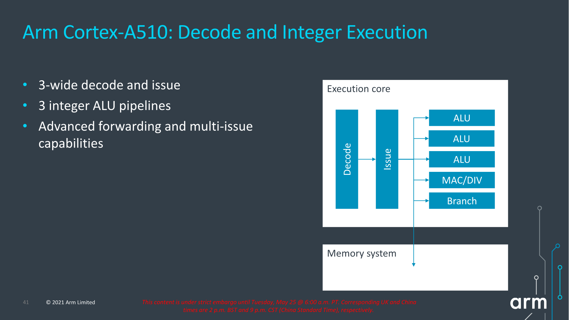
Although it’s an in-order architecture, Arm has still widened the back-end of the Cortex-A510 which now includes 3 ALUs, one complex MAC/DIV unit and a branch forwarding port. The explanation here is simply that there’s more opportunities to execute a wider variety of code blocks in fewer cycles when there’s a fitting sequence of instructions coming in to be executed.
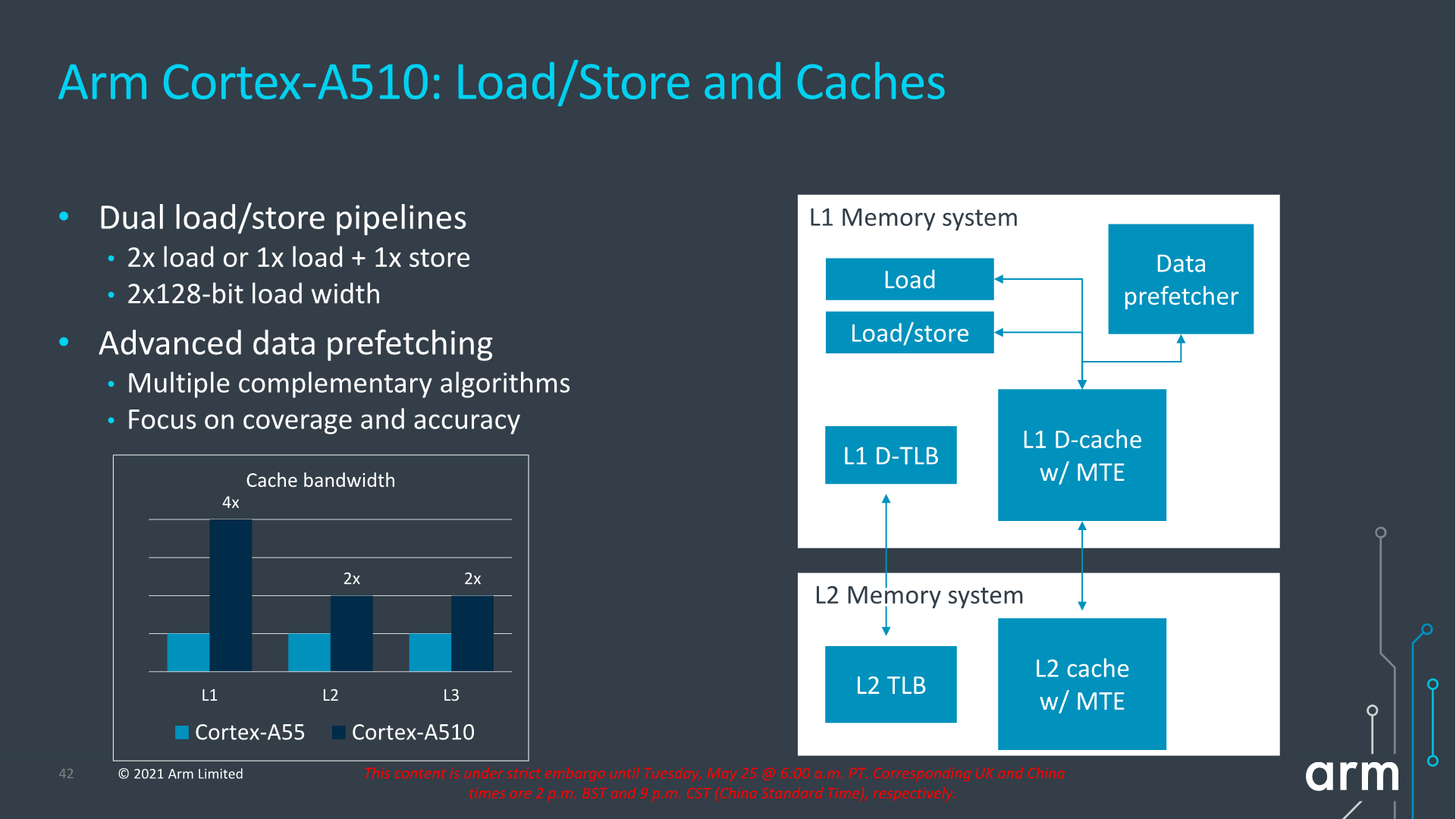
Finally, in the load-store system, the new structure is massively improved in comparison to the Cortex-A55 as we’re seeing a move from a load and store pipeline towards a load and a load/store pipeline, effectively doubling up on the number of loads executed per cycle. The width of the pipelines has also been increased with a doubling from 64b width to 128b width, so essentially load bandwidth compared to the Cortex-A55 is quadrupled.
The A510 also employs the similar very advanced prefetcher designs that we’ve seen in other recent big Arm cores, and adds to the large performance improvements that the core is able to achieve.
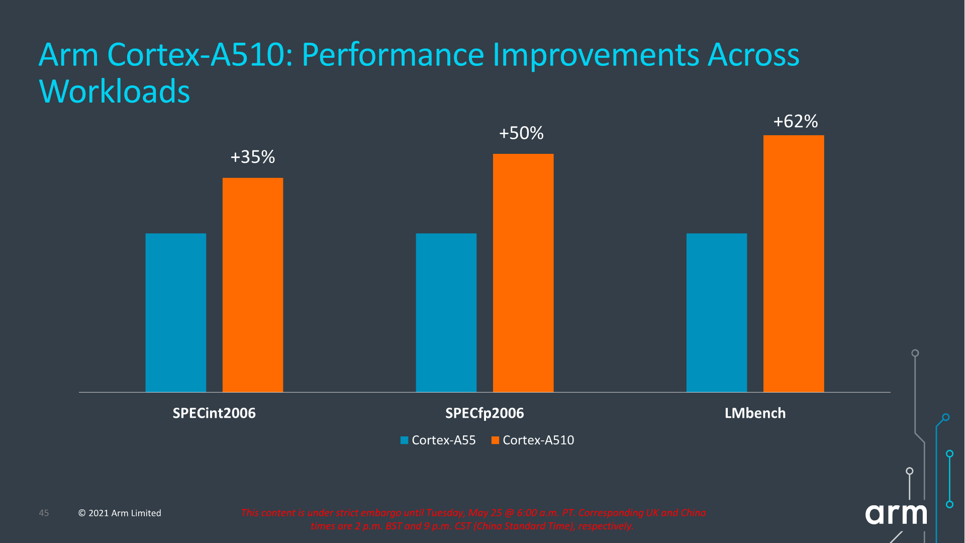
In terms of performance metrics, much like on the X2 and A710 presentation slides, the figures for the A510 aren’t very apples-to-apples as we’re comparing a Cortex-A55 with 32KB L1, 128KB L2 and 4MB L3 versus a Cortex-A510 with 32KB L1, 256KB L2 and 8MB L3. Frequency between the two cores is said to be the same. Under that scenario, we’re seeing +35% in SPECint2006 and +50% in SPECfp2006, which are seemingly very solid generational improvements, however given the cache hierarchy discrepancy as well as the fact that we’re comparing scores to a 4+ year old core, the actual improvements, especially from a compound annual growth rate (CAGR), doesn’t seem to be all that impressive.
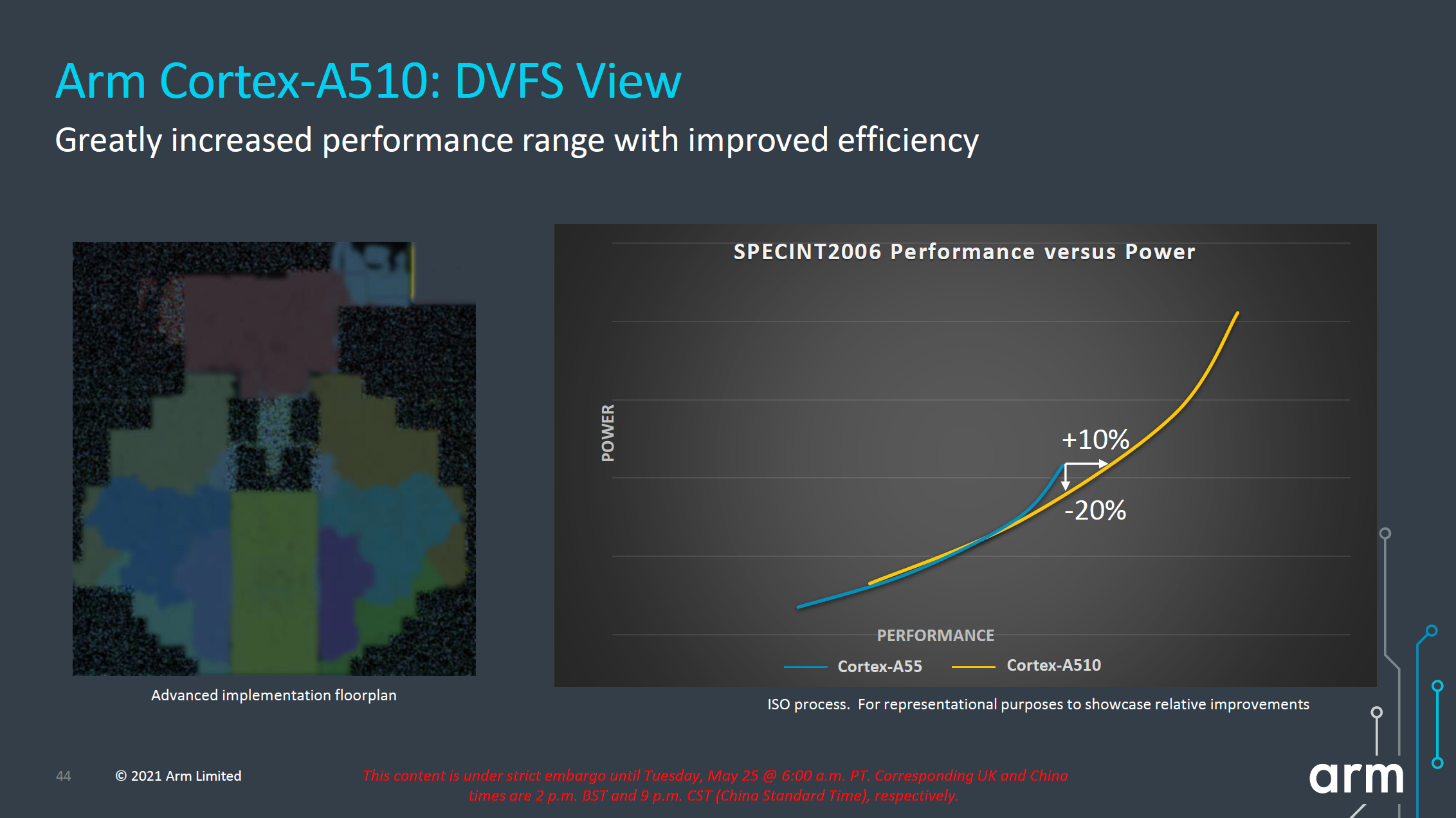
Looking at the projected performance and power curves on an ISO-process comparison, the new A510 seems rather lackluster from an efficiency standpoint. The ISO-power and ISO-performance gains are respectively +10% performance and -20% power, but the latter is really only valid for the high-end of the A55’s frequency curve, all the while the A510 pretty much overlaps the A55’s curve at lower operating points. While the A510 offers overall better performance, this seems to mostly be a product of extending the efficiency curve to higher power levels, and I was frankly disappointed to see this.
We’ll have to wait for the new generation SoCs to actually hit the market for us to test the new A510 cores, but if indeed they come with larger power consumption operating points to achieve higher performance, then Arm won't be much nearer in catching up to what Apple has been doing with their efficiency cores. As of the latest generation of SoCs, Apple’s efficiency cores were around 4x faster than any Cortex-A55 based SoC. Which, running at roughly the same system active power, also made them 3-4x more efficient in the traditional benchmarks. As presented, a theoretical A510 SoC won't be able to close that efficiency gap at all.
Arm is still adamant that for the kind of general use-cases in which the little cores are used in mobile phones – such as very light UI workloads – that their little core approach is still the most power-efficient way to achieve the best “DoU” or days of use figures. This is based in part on their internal projections as well as their partners', all of which indicate that the the triple issue in-order design they've developed is the most efficient option.
As the team explains it, it’s actually extremely hard to reproduce these more real-world workloads in any more structured benchmark (such as the typical test suites we tend to employ), but admitted there’s no real alternative that one could use to isolate performance and efficiency in such tasks. Generally, my counter-argument here is that iPhones still have outstanding battery life, so I’m still extremely skeptical on the whole lower-performance in-order core approach versus a more efficiency focused OOO core as demonstrated by Apple. Especially since we don’t really have an independent way to really test Arm’s claims, and the only data points we do have paint a very different picture.
Arm does note that this generation also had a lot of work done in regards to architectural features, and that the A510 is merely a starting point in a series of generations that are planned to be updated in a more regular fashion versus the large 4–5-year gap we’ve seen with the Cortex-A55 (just to be explicit, Arm doesn’t promise yearly updates, but we’ll be seeing successors in a much faster timeline). Those successors will see continued improvements in performance and power efficiency.
For this upcoming generation, the one benefit of the new little cores will come in more mixed-load workloads. Due to the DVFS nature of the various cores in an SoC, with most core groups sharing the same voltage rail, the A510 little cores represent an overall more efficient execution path. Besides their immediate simplicity, they generally operate at a lower voltage, further boosting their energy savings over using the more performant but power hungry middle cores. Which means that if there are any workloads that previously couldn't be sufficiently serviced by the A55 cores – but now can by the A510 cores – then those workloads would see a big jump in execution efficiency.
Overall, I’m still feeling a bit underwhelmed by the new A510 core, particularly given the 4 years it took to design it. Let’s hope that the upcoming mobile SoCs will have more apparent efficiency to them when we're testing them in 2022 devices.
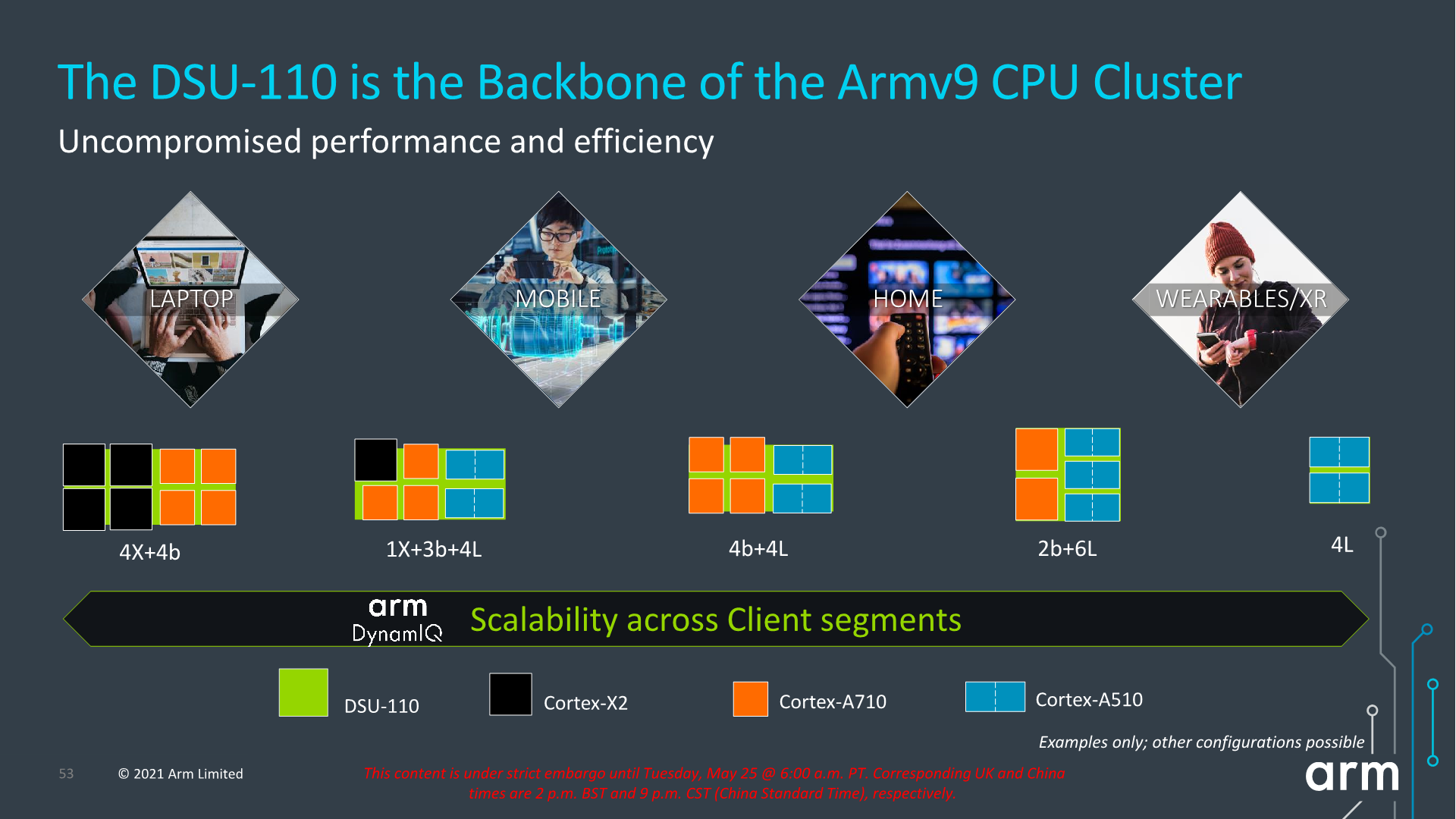
Alongside the new CPU microarchitectures, Arm today is also announcing a new L3 design in the form of the new DSU-110. The “DynamIQ Shared Unit” had been the company’s go-to cluster and “core complex” block ever since it was introduced in 2017 with the Cortex-A75 and Cortex-A55. While we’ve seen small iterative improvements, today’s DSU-110 marks a major change in how the DSU operates and how it promises to scale up in cache size and bandwidth.
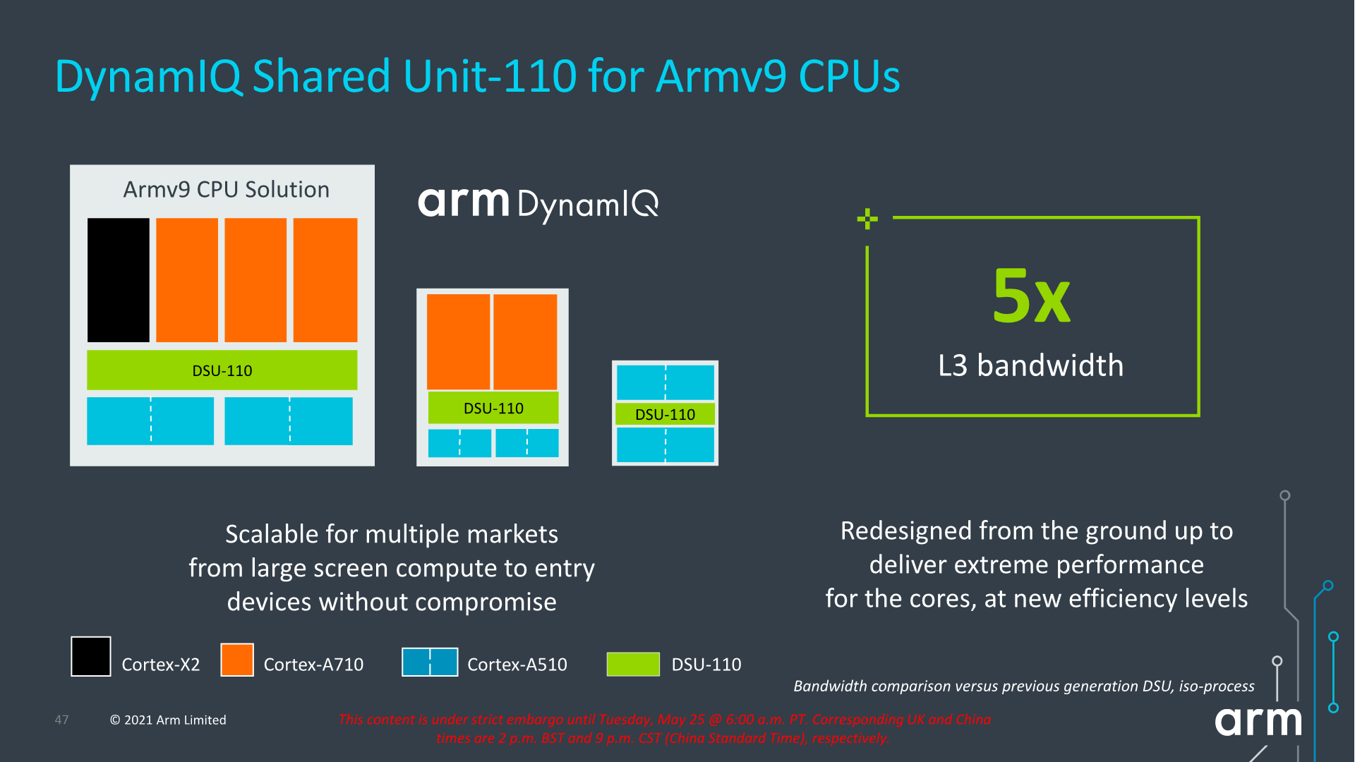
The new DSU-110 is a ground-up redesign with an emphasis on more bandwidth and more power efficiency. It continues to be the core building block for all of Arm’s mobile and lower tier market segments.
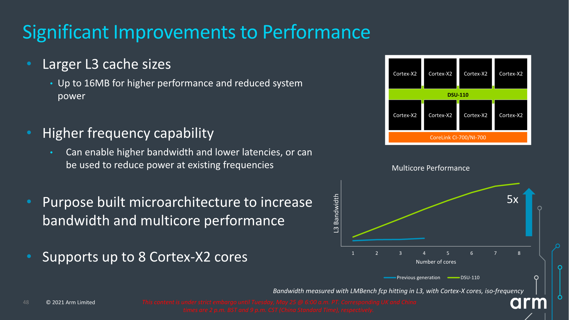
A key metric is of course the increase of L3 cache configuration which will now go up to 16MB this generation. This is of course the high-end of the spectrum and generally we shouldn’t expect such a configuration in a mobile SoC soon, but Arm has had several slides depicting larger form-factor implementations using such a larger design housing up to 8 Cortex-X2 cores. This is undoubtedly extremely interesting for a higher-performance laptop use-case.
The bandwidth increase of the new design is also significant, and applies from single-thread to multi-threaded scenarios. The new DSU-110 promises aggregate bandwidth increases of up to 5x compared to the contemporary design. More interesting is the fact that it also significantly boosts single-core bandwidth, and Arm here actually notes that the new DSU can actually support more bandwidth than what’s actually capable of the new core microarchitectures for the time being.
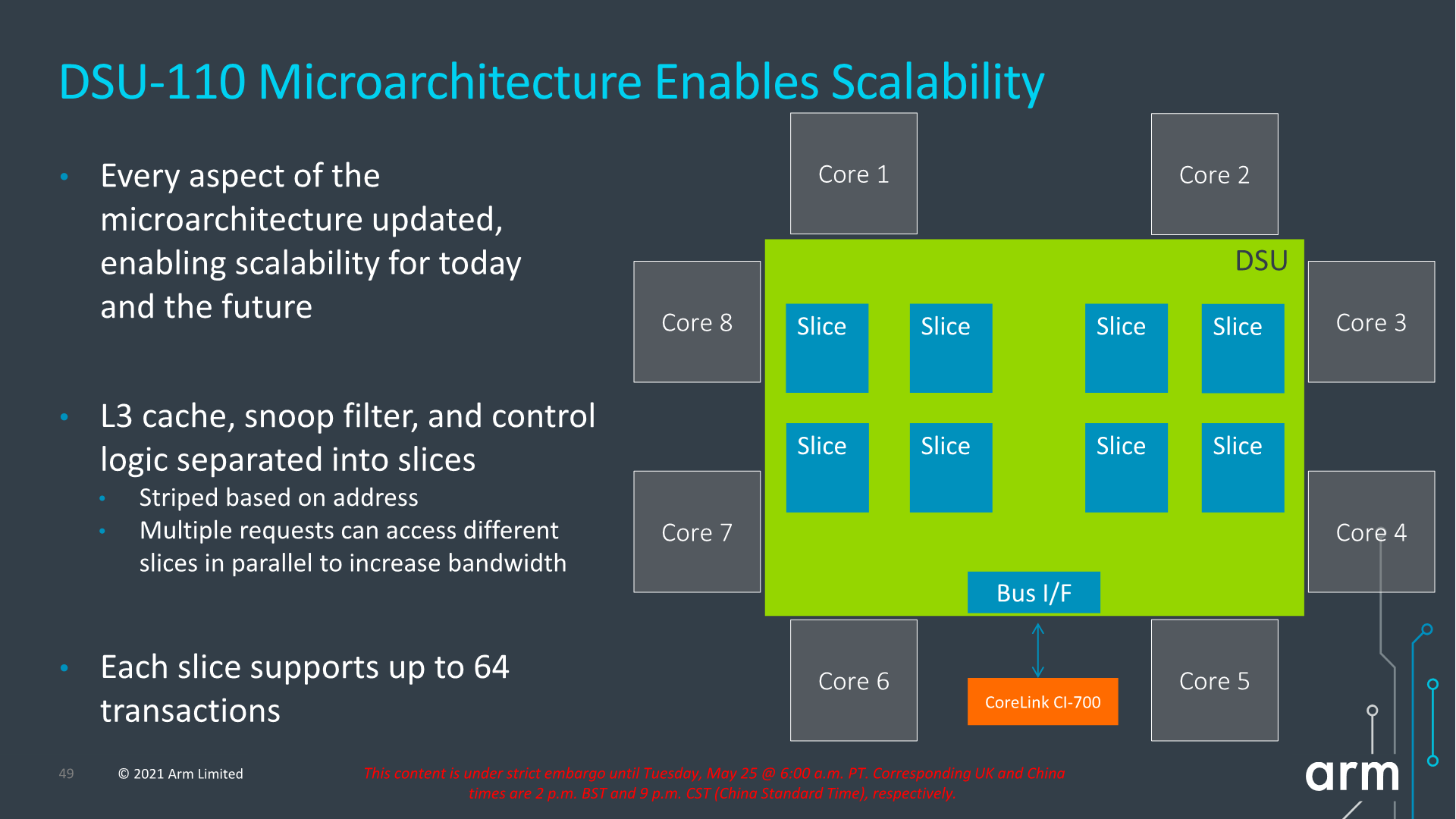
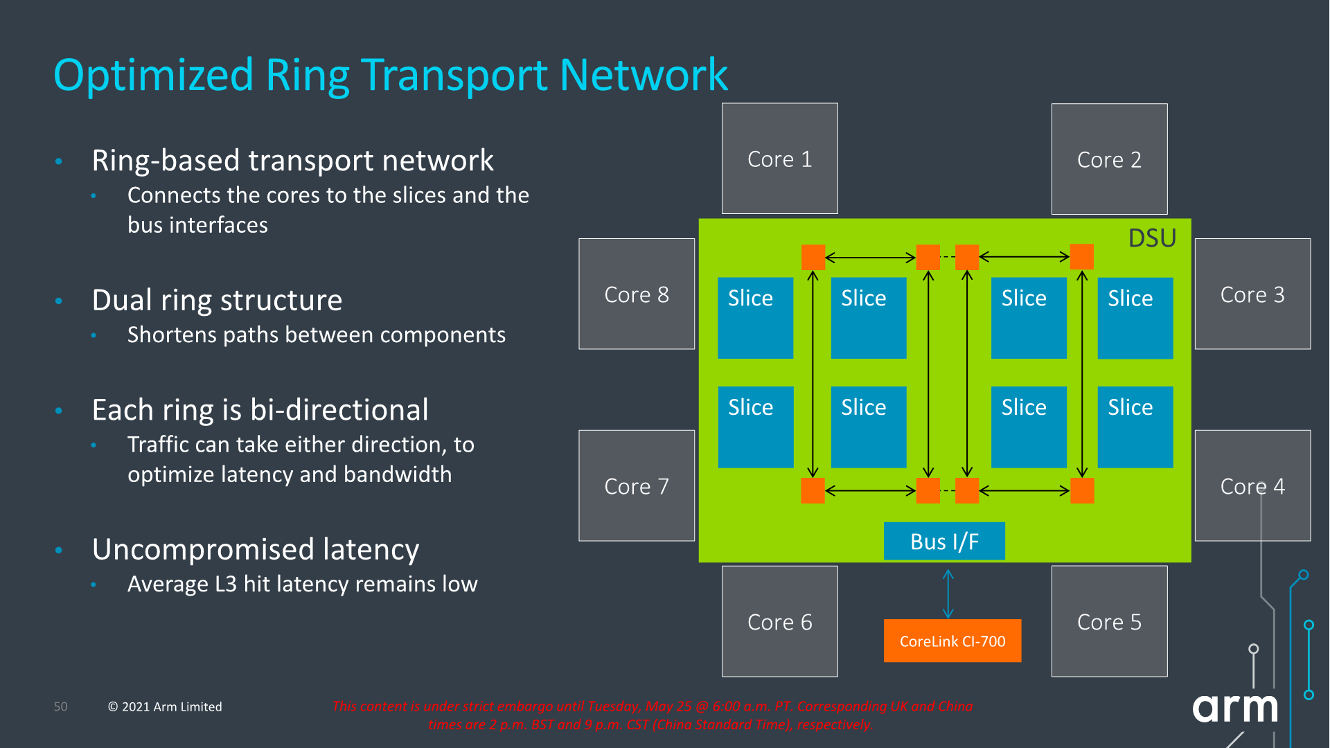
Arm never really disclosed the internal topology of the previous generation DSU, but remarks that with the DSU-110 the company has shifted over to a bi-directional dual-ring transport topology, each with four ring-stops, and now supporting up to 8 cache slices. The dual-ring structure is used to reduce the latencies and hops between ring-stops and in shorten the paths between the cache slices and cores. Arm notes that they’ve tried to retain the same lower access latencies as on the current generation DSU (cache size increases aside), so we should be seeing very similar average latencies between the two generations.
Parallel access increases for bandwidth as well as more outstanding transactions seem to have been also very important in order to improve performance, which seems very exciting for upcoming SoC designs, but also puts into more question the previously presented CPU IPC improvements and exactly how much the new DSU-110 contributes to those numbers.
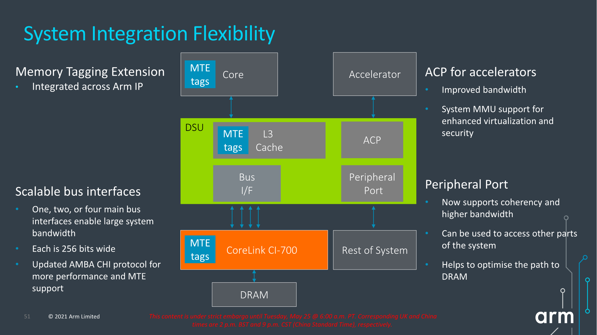
Architecturally, one important change to the capabilities of the DSU-110 is support for MTE tags, a upcoming security and debugging feature promising to greatly help with memory safety issues.
The new DSU can scale up to 4x AMBA CHI ports, meaning we’ll have up to 1024-bit total bi-directional bandwidth to the system memory. With a theoretical DSU clock of around 2GHz this would enable bandwidth of up to 256GB/s reads or writes, or double that when combined, plenty enough to be able to saturate also eventual high-end laptop configurations.

In terms of power efficiency, the new DSU offers more options for low-power operation when in idle situations, implementing partial L3 power-down, able to reduce leakage power of up to 75% compared to the current DSU.
In general idle situations but still having the full L3 powered on, the new design promises up to 25% reduction in leakage power all whilst offering 2x the bandwidth capabilities.
It’s important to note that we’re talking about leakage power here- active dynamic power is expected to generally scale linearly with the bandwidth increase of the new design, meaning 5x the bandwidth would also cost 5x the power. This would be an important factor to note into system power and in general the expected power behaviour of the next-gen SoCs when they’re put under heavy memory workloads.
Arm describes the DSU-110 as the backbone of the Armv9 cluster and that seemingly seems to be an apt description. The new bandwidth capabilities are sure to help out both with single-threaded, but also with multi-threaded performance of upcoming SoCs. Generally, the new 16MB L3 capability, while it’s possible somebody might do a high-end laptop SoC configuration, isn’t as exciting as the now finally expected move to a new 8MB L3 on mobile SoCs, hopefully also enabling higher power efficiency and more battery life for devices.
Finally, the last new announcement of the day is a new interconnect and network-on-chip generation. The last time Arm had announced a mobile/client interconnect was back in in 2015 with the CCI-550. The reason for the large gap between IPs, in Arm’s own words, is that ever since Arm’s introduction of the DSU in its CPU complexes, there really hasn’t been any need for a cache coherent interconnect in the market. While that’s eyebrow-raising from a GPU perspective, it makes perfect sense from a CPU perspective, as coherency between CPU cores was the primary driver for such interconnects until then.
With the advent of new more complex computing platforms, such as NPUs, accelerators, and hopeful more use of GPUs in cache-coherent fashions, Arm saw a need gap in its portfolio and decided to update its client-side interconnect IP.
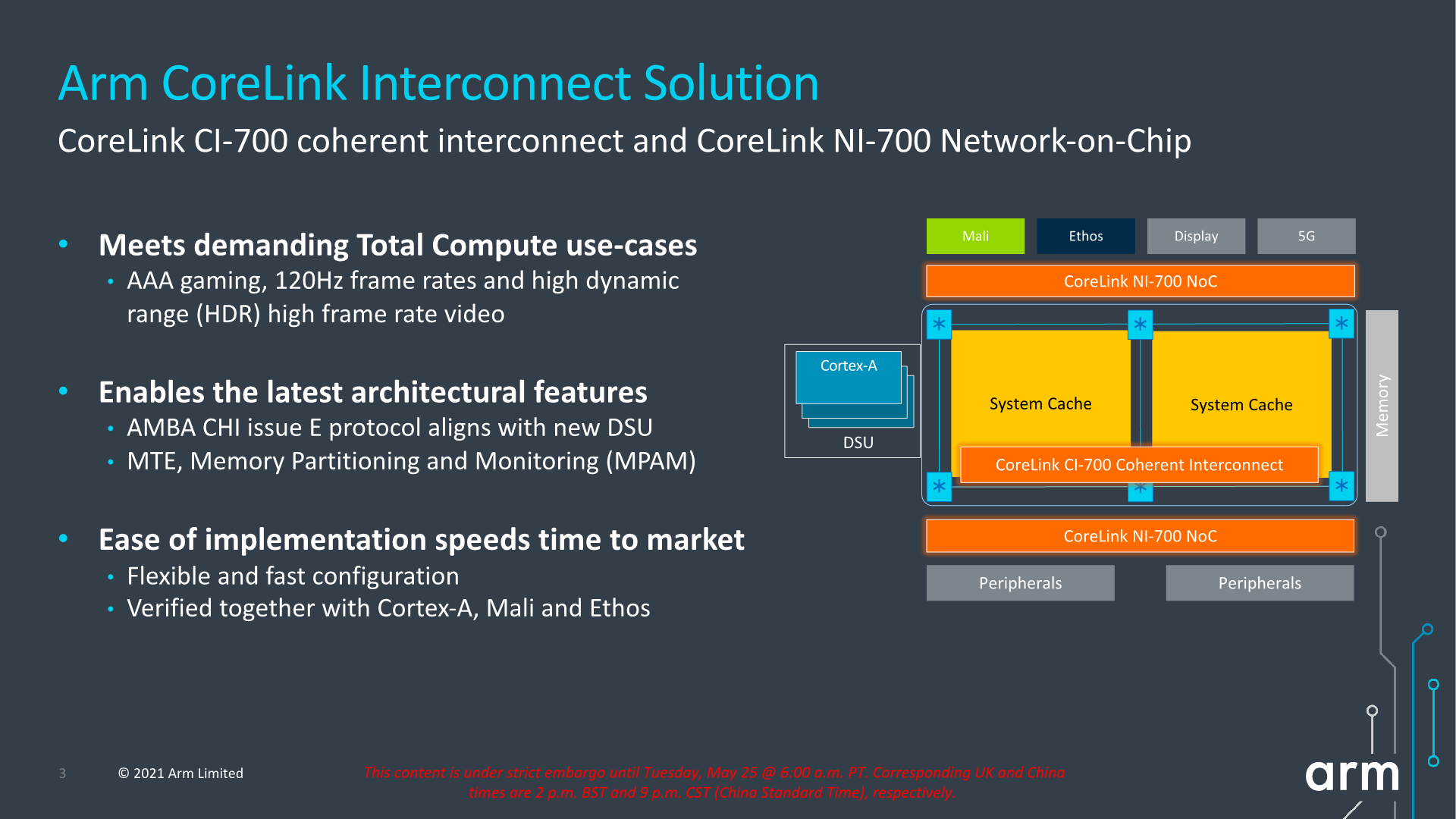
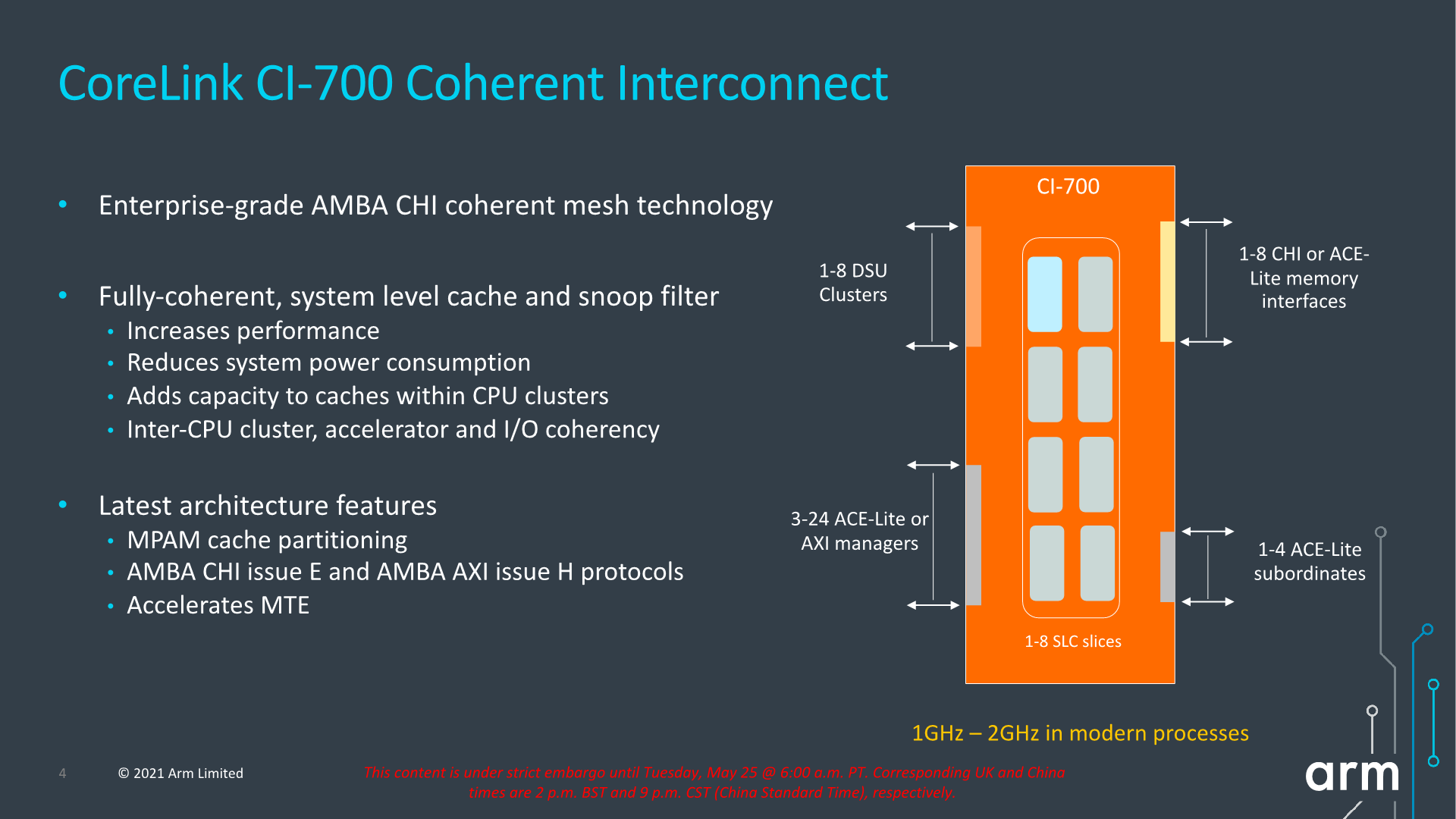
The new CI-700 is a mobile and client optimised variant of Arm’s infrastructure CMN mesh network, implementing important new interoperability with the new IP announced today, such as the new DSU or CPU cores.
The new mesh interconnect scales up from 1 to 8 DSU clusters, and supports up to 8 memory controllers, and also introduces innovations such as a system level cache.
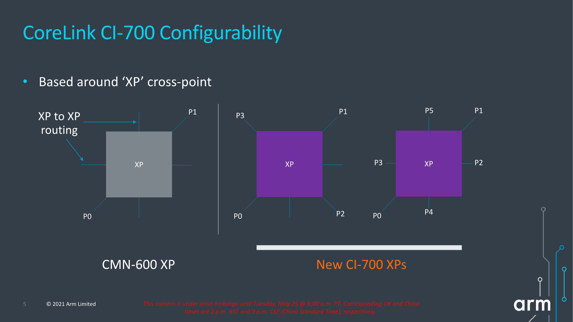
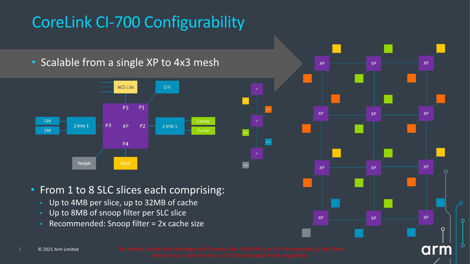
The mesh network topology and building blocks is very similar to what we’ve seen in the CMN infrastructure IP, in that “points” in the mesh are comprised of “cross-points” or “XP”. One differentiation that’s unique to the client mesh implementation is that XPs can have more attached connectivity ports, trading in routing connection paths. The new IP can also be configured as just a sole XP with no real mesh so to speak of, or essentially a 1x1 mesh configuration. This can grow up to a 4x3 mesh in the largest possible configuration.
The mesh supports from 1 to 8 SLC slices, with up to 4MB per slice for a total of 32MB, and snoop filter SRAM with coverage of up to 8MB address space per slice. It’s noted that generally Arm recommends 1.5-2x of coverage of the underlying private cache hierarchies of the mesh clients.
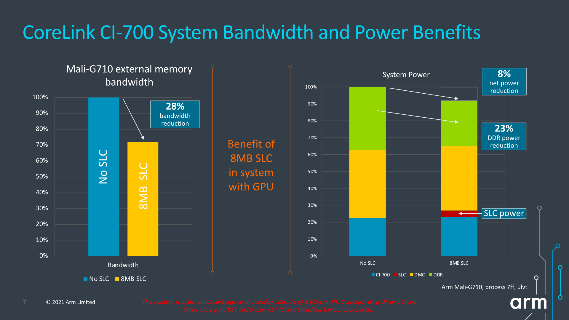
The SLC can server as both a bandwidth amplifier as well as reducing external memory/DRAM transactions, reducing system power reduction.
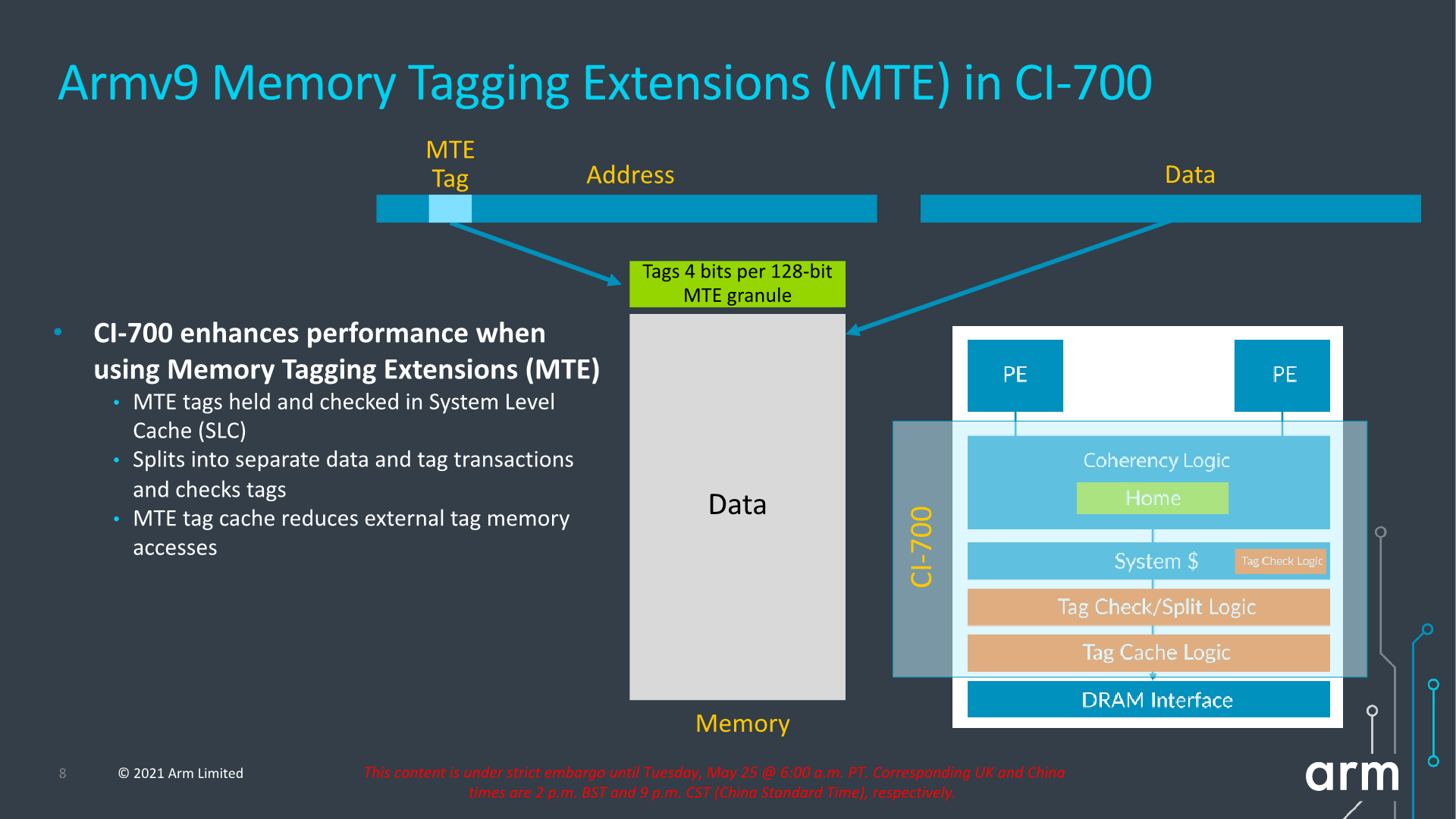
We see a reiteration of the support for MTE, allowing for this generation of IPs to support the feature across the new CPU IP, the DSU, and the new cache coherent interconnect.
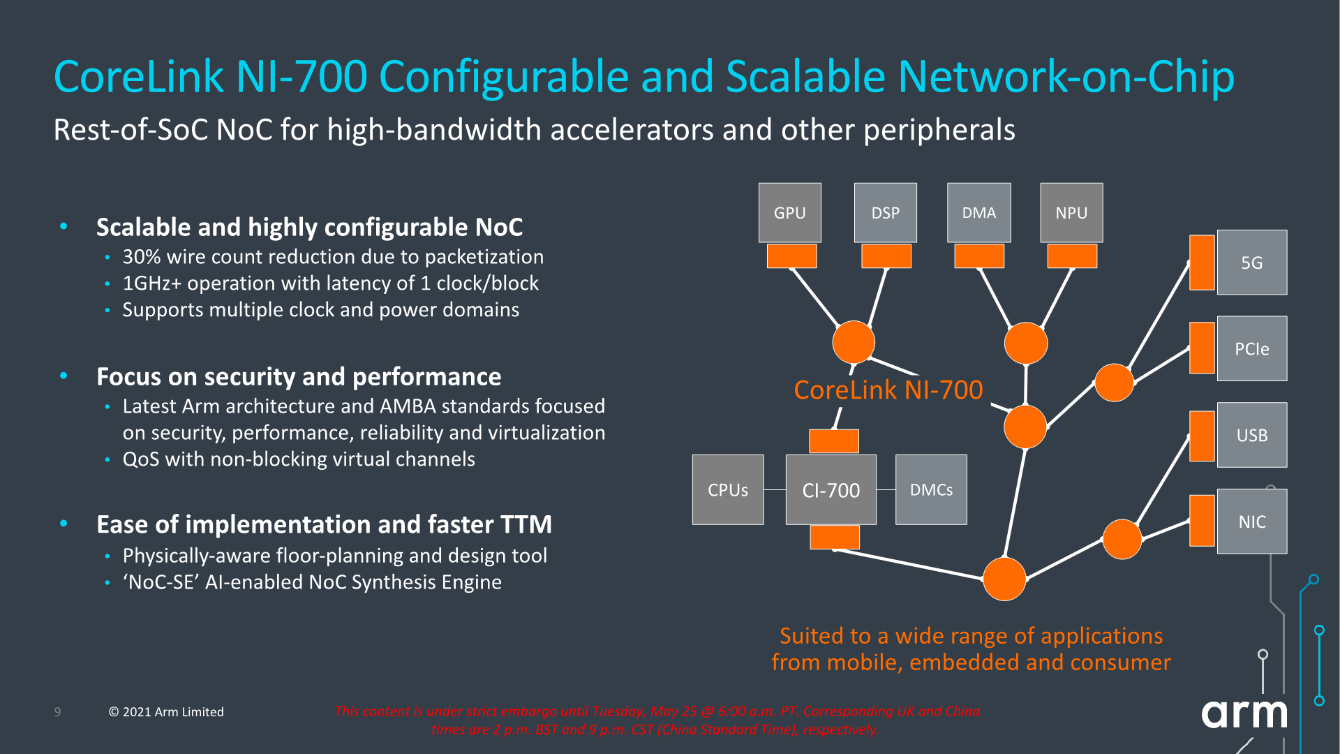
Alongside the new CI-700 coherent interconnect, we’re also seeing a new NI-700 network-on-chip for non-coherent data transfers between a SoC’s various IP blocks. The big new improvements here is the introduction of packetization for data transfers, which leads to a reduction of wires and thus improves area efficiency of the NoC on the SoC.
Overall, the new system IP announced today is very interesting, but the one question that’s one has to ask oneself is exactly who these net interconnects are meant for. Over the last few years, we’ve seen essentially every major mobile vendor roll out their own in-house cache-coherent interconnect IP, such as Samsung’s SCI or MediaTek’s MCSI, and other times we don’t see vendors talk about their in-house interconnects at all (Qualcomm). Due to almost everybody having their own IP, I’m not sure what the likelihood would be that any of the big players would jump back to Arm’s own solutions – if somebody were to adopt it, it would rather be amongst the smaller name vendors and newcomers to the market. From a business and IP portfolio perspective, the new designs make a lot of sense and allows to have the building blocks to create a mostly Arm-only SoC, which is an important item to have on the menu for Arm’s more diverse customer base.
Today’s Arm Client TechDay disclosures were generally quite a lot more extensive than in the last few years, especially given the number of new IP releases we’ve covered. Three new CPU microarchitectures, a new DSU/L3 cluster design, and two new SoC interconnect IPs is quite a bit more than we’re used to, and it goes to underscore just how much effort Arm is putting into updating all of the parts of its client IP.
Starting off with the CPUs, the new Cortex-X2 and Cortex-A710 cores are meant to be iterative designs compared to their predecessors, and that's certainly what they are from a performance and efficiency viewpoint. On a generational basis, Arm is promising a 10-16% improvement in IPC. However these figures are somewhat muddled by the fact we’re also comparing 4MB and 8MB L3 caches. Generally, it’s a reasonable expectation of what we’ll be seeing in 2022 devices, but it’s also hard to disambiguate and attribute the performance of the cores versus that of the new DSU-110 L3 cluster design.
Arm has also made some more lofty performance claims when it comes to actual device implementations in 2022, such as +30% peak-to-peak performance boosts on the parts of the X2 cores. Generally, given our expectations that both the next Snapdragon and the next Exynos flagships will come in a similar Samsung foundry process node with smaller improvements, I’m very doubtful we’ll be seeing such larger generational improvements in practice, unless somehow MediaTek surprises us with a flagship X2 SoC made out at TSMC.
While the X2 and A710 aren’t all that groundbreaking, we have to note that the move towards Armv9 brings a lot of new architectural features that would otherwise eat into the expected yearly performance or efficiency improvements. The move to the new ISA baseline has been a long time coming and I’m curious to see what it will enable in terms of media applications (SVE) or AI (new ML instructions).
This is also the fourth and last iteration of Arm’s Austin core family, so hopefully next year’s new Sophia family will see larger generational leaps. Arm admits that we’re nearing diminishing returns and it’s certainly not at the same break-neck pace it was moving a few years ago, but there’s still a lot which can be done.
Today we also saw the unveiling of a brand-new little core in the form of the Cortex-A510. A new clean-sheet design from the Cambridge team, it’s certainly using an innovative approach given its “merged core” design, sharing the L2 cache hierarchy and the FP/SIMD back-end amongst two otherwise full featured cores. The performance and IPC gains are claimed to be quite large at +35-50%, however it seems that this generation hasn’t improved the efficiency curve all that much. It’s still a much better design and will have effective benefits for power efficiency in real-world workloads due to how workloads interact between the little and larger cores, but leaves us with a feeling that it doesn’t provide a knock-out convincing jump we had expected after 4 years. The silver lining here is that Arm is promising further generational improvements in performance and power with subsequent iterations, so we won’t be left with the current state of affairs the same way we saw the Cortex-A55 stagnate.
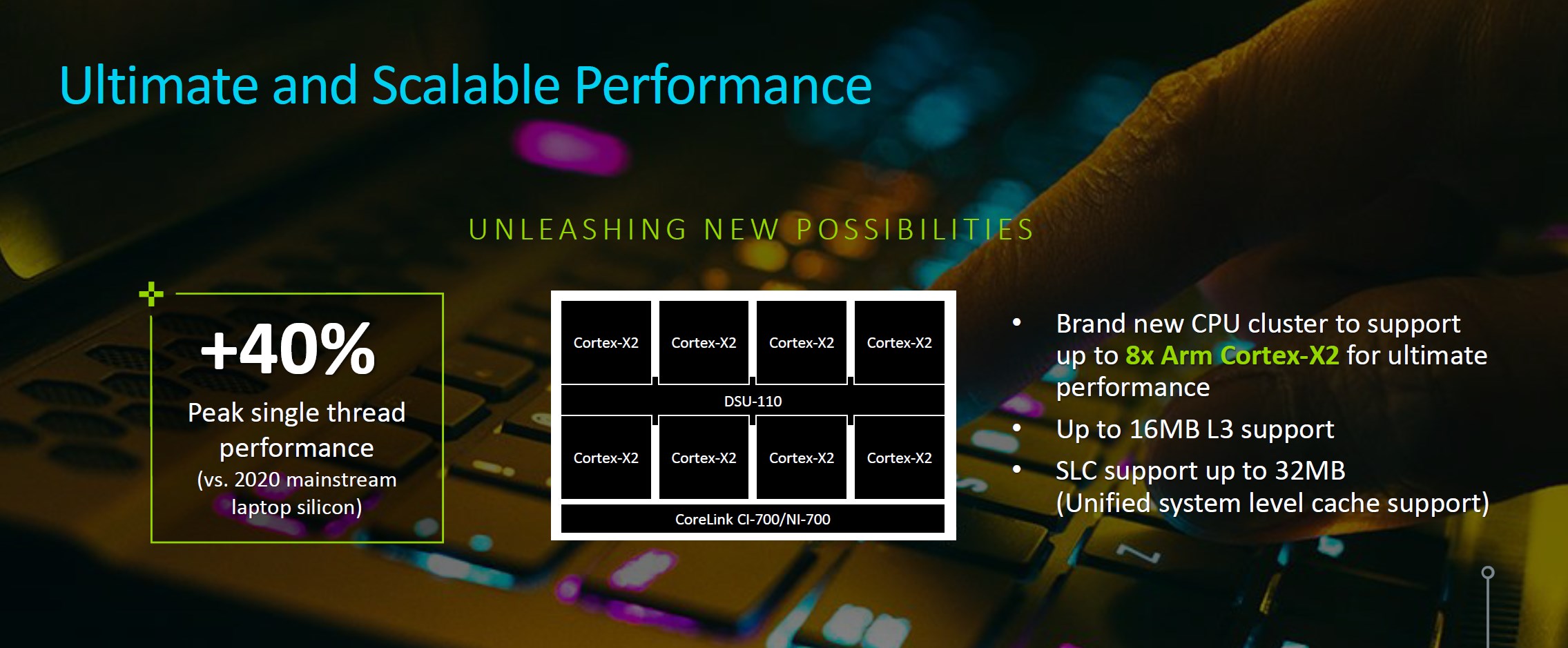
One of the more key points I saw Arm put their focus on was the new possibilities in larger form-factor devices beyond mobile. The new DSU-110 now supports up to 8 Cortex-X2 cores, a theoretical setup that would pretty much blow away the current Cortex-A76 based Arm laptop SoCs such as the Snapdragon 8cx family. The new cluster design allows for large L3 caches of up to 16MB, and while I don’t know if we’ll see the new interconnect IPs used by the larger vendors, it surely also makes a big argument for larger performance designs. The catch is that if Qualcomm were to adopt and make such a design, it would seemingly be short-lived given their recent Nuvia acquisition and intent on using custom cores. Otherwise, because of a lack of Mali Windows drivers, this really only leaves space for a theoretical Samsung laptop SoC with AMD RDNA GPU, but such a SoC could nonetheless be very successful.
Overall, this year’s CPU and system IP announcements from Arm are extremely solid new IP offerings, really laying down a new foundation, both architecturally with Armv9, and microarchitecturally thanks to elements such as the new DSU and the new little core CPUs. We’re looking forward to the new 2022 SoCs and products that will be powered by the new Arm IP.
Technology - Latest - Google News
May 25, 2021 at 09:00PM
https://ift.tt/3yCtBFj
Arm Announces Mobile Armv9 CPU Microarchitectures: Cortex-X2, Cortex-A710 & Cortex-A510 - AnandTech
Technology - Latest - Google News
https://ift.tt/2AaD5dD
Bagikan Berita Ini


0 Response to "Arm Announces Mobile Armv9 CPU Microarchitectures: Cortex-X2, Cortex-A710 & Cortex-A510 - AnandTech"
Post a Comment